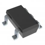
IPS521 High Side Power Mosfet Switch transistor socket 3 pin Fully Protected
|
|
Features • Over temperature protection (with auto-restart) • Short-circuit protection (current limit) • Active clamp • E.S.D protection • Status feedback • Open load detection • Logic ground isolated from power ground IPS521/IPS521S Data Sheet No.PD 60158-H
Description The IPS521/IPS521S are fully protected five terminal high side switches with built in short-circuit , overtemperature, ESD protection, inductive load capability and diagnostic feedback. The output current is controlled when it reaches Ilim value. The current limitation is activated until the thermal protection acts. The over-temperature protection turns off the high side switch if the junction temperature exceeds Tshutdown. It will automatically restart after the junction has cooled 7o C below Tshutdown. A diagnostic pin is provided for status feedback of short-circuit, over-temperature and open load detection. The double level shifter circuitry allows large offsets between the logic ground and the load ground.
Recommended Operating Conditions These values are given for a quick design. For operation outside these conditions, please consult the application notes
Lead Assignments
|
||||||||||||||||||||||||||||||||||||
| Product Tags: npn smd transistor multi emitter transistor |