
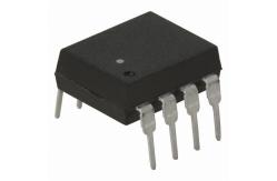
HCNR201 Integrated Circuit Chip High-Linearity Analog Optocouplers
|
|
Description The HCNR200/201 high-linearity analog optocoupler consists of a high-performance AlGaAs LED that illuminates two closely matched photodiodes. The input photodiode can be used to monitor, and therefore stabilize, the light output of the LED. As a result, the non-linearity and drift characteristics of the LED can be virtually eliminated. The output photodiode produces a photocur rent that is linearly related to the light output of the LED. The close matching of the photo-diodes and advanced design of the package ensure the high linearity and stable gain characteristics of the opto coupler.
The HCNR200/201 can be used to isolate analog signals in a wide variety of applications that require good stability, linearity, bandwidth and low cost. The HCNR200/201 is very fl exible and, by appro priate design of the application circuit, is capable of operating in many diff erent modes, includ ing: unipolar/bipolar, ac/dc and inverting/ non-inverting. The HCNR200/201 is an excellent solution for many analog isola tion problems.
Features Low nonlinearity: 0.01% K3 (IPD2/IPD1) transfer gain HCNR200: ±15% HCNR201: ±5% Low gain temperature coeffi cient: -65 ppm/°C Wide bandwidth – DC to >1 MHz Worldwide safety approval – UL 1577 recognized (5 kV rms/1 min rating) – CSA approved – IEC/EN/DIN EN 60747-5-2 approved VIORM = 1414 V peak (option #050) Surface mount option available (Option #300) 8-Pin DIP package - 0.400” spacing Allows fl exible circuit design
Package Outline Drawings
Absolute Maximum Ratings Storage Temperature ..............................................................................................-55°C to +125°C Operating Temperature (TA) ................................................................................. -55°C to +100°C Junction Temperature (TJ ) ......................................................................................................... 125°C Refl ow Temperature Profi le ..............................................See Package Outline Drawings Section Lead Solder Temperature ............................................................................................260°C for 10s (up to seating plane) Average Input Current - IF ........................................................................................................ 25 mA Peak Input Current - IF ............................................................................................................... 40 mA (50 ns maximum pulse width) Reverse Input Voltage - VR ............................................................................................................2.5 V (IR = 100 μA, Pin 1-2) Input Power Dissipation .................................................................................... 60 mW @ TA = 85°C (Derate at 2.2 mW/°C for operating temperatures above 85°C) Reverse Output Photodiode Voltage ........................................................................................30 V (Pin 6-5) Reverse Input Photodiode Voltage ............................................30 V (Pin 3-4) |
| Product Tags: electronic integrated circuit digital integrated circuits |
|
RB450FT106 Rectifier Diode Schottky barrier diode diode laser hair removal |
|
TK10P60W Power Mosfet Transistor MOSFETs Silicon N-Channel MOS |
|
4N25M Electronic IC Chips General Purpose Phototransistor Optocouplers |
|
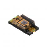
TEMT6000X01 Electronic IC Chips Ambient Light Sensor, RoHS Compliant |
|
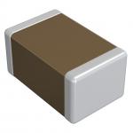
GRM033R71C272KA88D NEW AND ORIGINAL STOCK |
|
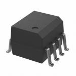
FOD2742B Flash Memory IC NEW AND ORIGINAL STOCK |