
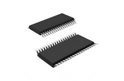
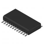
CY7C68013A-100AXC Integrated Circuit Chip EZ-USB FX2LP USB Microcontroller
|
|
CY7C68013A/CY7C68014A CY7C68015A/CY7C68016A EZ-USB FX2LP™ USB Microcontroller
1.0 Features (CY7C68013A/14A/15A/16A)
• USB 2.0–USB-IF high speed certified (TID # 40440111) • Single-chip integrated USB 2.0 transceiver, smart SIE, and enhanced 8051 microprocessor • Fit, form and function compatible with the FX2 — Pin-compatible — Object-code-compatible — Functionally-compatible (FX2LP is a superset)
• Ultra Low power: ICC no more than 85 mA in any mode — Ideal for bus and battery powered applications • Software: 8051 code runs from: — Internal RAM, which is downloaded via USB — Internal RAM, which is loaded from EEPROM — External memory device (128 pin package)
• 16 KBytes of on-chip Code/Data RAM • Four programmable BULK/INTERRUPT/ISOCHRONOUS endpoints — Buffering options: double, triple, and quad • Additional programmable (BULK/INTERRUPT) 64-byte endpoint • 8- or 16-bit external data interface • Smart Media Standard ECC generation
• GPIF (General Programmable Interface) — Allows direct connection to most parallel interface — Programmable waveform descriptors and configuration registers to define waveforms — Supports multiple Ready (RDY) inputs and Control (CTL) outputs
• Integrated, industry-standard enhanced 8051 — 48-MHz, 24-MHz, or 12-MHz CPU operation — Four clocks per instruction cycle — Two USARTS — Three counter/timers — Expanded interrupt system — Two data pointers
• 3.3V operation with 5V tolerant inputs • Vectored USB interrupts and GPIF/FIFO interrupts • Separate data buffers for the Set-up and Data portions of a CONTROL transfer • Integrated I2C controller, runs at 100 or 400 kHz
• Four integrated FIFOs — Integrated glue logic and FIFOs lower system cost — Automatic conversion to and from 16-bit buses — Master or slave operation — Uses external clock or asynchronous strobes — Easy interface to ASIC and DSP ICs
1.1 Features (CY7C68013A/14A only)
• CY7C68014A: Ideal for battery powered applications — Suspend current: 100 µA (typ) • CY7C68013A: Ideal for non-battery powered applications — Suspend current: 300 µA (typ) • Available in four lead-free packages with up to 40 GPIOs — 128-pin TQFP (40 GPIOs), 100-pin TQFP (40 GPIOs), 56-pin QFN (24 GPIOs) and 56-pin SSOP (24 GPIOs)
1.2 Features (CY7C68015A/16A only)
• CY7C68016A: Ideal for battery powered applications — Suspend current: 100 µA (typ) • CY7C68015A: Ideal for non-battery powered applications — Suspend current: 300 µA (typ) • Available in lead-free 56-pin QFN package (26 GPIOs) — 2 more GPIOs than CY7C68013A/14A enabling additional features in same footprint
Cypress Semiconductor Corporation’s (Cypress’s) EZ-USB FX2LPTM (CY7C68013A/14A) is a low-power version of the EZ-USB FX2TM (CY7C68013), which is a highly integrated, low-power USB 2.0 microcontroller. By integrating the USB 2.0 transceiver, serial interface engine (SIE), enhanced 8051 microcontroller, and a programmable peripheral interface in a single chip, Cypress has created a very cost-effective solution that provides superior time-to-market advantages with low power to enable bus powered applications.
The ingenious architecture of FX2LP results in data transfer rates of over 53 Mbytes per second, the maximum-allowable USB 2.0 bandwidth, while still using a low-cost 8051 microcontroller in a package as small as a 56 QFN. Because it incorporates the USB 2.0 transceiver, the FX2LP is more economical, providing a smaller footprint solution than USB 2.0 SIE or external transceiver implementations. With EZ-USB FX2LP, the Cypress Smart SIE handles most of the USB 1.1 and 2.0 protocol in hardware, freeing the embedded microcontroller for application-specific functions and decreasing development time to ensure USB compatibility.
The General Programmable Interface (GPIF) and Master/Slave Endpoint FIFO (8- or 16-bit data bus) provides an easy and glueless interface to popular interfaces such as ATA, UTOPIA, EPP, PCMCIA, and most DSP/processors.
The FX2LP draws considerably less current than the FX2 (CY7C68013), has double the on-chip code/data RAM and is fit, form and function compatible with the 56-, 100-, and 128- pin FX2.
Four packages are defined for the family: 56 SSOP, 56 QFN, 100 TQFP, and 128 TQFP.
2.0 Applications
• Portable video recorder • MPEG/TV conversion • DSL modems • ATA interface • Memory card readers • Legacy conversion devices • Cameras • Scanners • Home PNA • Wireless LAN • MP3 players • Networking
Absolute Maximum Ratings
Storage Temperature ...........................................................................................–65°C to +150°C Ambient Temperature with Power Supplied..................................................................0°C to +70°C Supply Voltage to Ground Potential...........................................................................–0.5V to +4.0V DC Input Voltage to Any Input Pin ........................................................................................... 5.25V DC Voltage Applied to Outputs in High Z St...................................................... –0.5V to VCC + 0.5V Power Dissipation ................................................................................................................ 300 mW Static Discharge Voltage ..................................................................................................... > 2000V Max Output Current, per I/O port ............................................................................................ 10 mA Max Output Current, all five I/O ports (128- and 100-pin packages) ........................................ 50 mA
Operating Conditions
TA (Ambient Temperature Under Bias) .......................................................................0°C to +70°C Supply Voltage ......................................................................................................+3.15V to +3.45V Ground Voltage............................................................................................................................ 0V FOSC (Oscillator or Crystal Frequency)................................................................ 24 MHz ± 100 ppm ............................................................................................................................... Parallel Resonant
Block Diagram
|
| Product Tags: electronic integrated circuit digital integrated circuits |
|
BTS724GXUMA1 Smart High-Side Power Switch Four Channels programmed integrated led circuit board |
|
TPS61041DBVR Electronic IC Chips LOW-POWER DC/DC BOOST CONVERTER |
|
US90AEVK Electronic IC Chips power ic chip 24V Hall IC Fan Driver |
|
TLE4226G Integrated Circuit Chip Intelligent Sixfold Low-Side Switch |
|
NCP1234AD65R2G Fixed Frequency Current Mode Controller for Flyback Converters |
|
REG1117FA-5.0 Integrated Circuit IC Chip Low Dropout Positive Regulator |