China Flash Memory IC Chip manufacturer
ChongMing Group (HK) Int'l Co., Ltd
CHONGMING GROUP (HK) INT'L CO., LTD.
3
Home > Products > Integrated Circuit Chips >

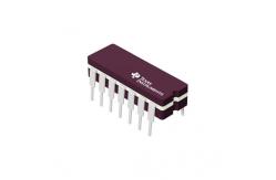
SN74HC04N Electronic IC Chips integrated components Hex inverter

Browse Categories

ChongMing Group (HK) Int'l Co., Ltd

City: shenzhen

Country/Region:china

Tel:86-755-88367702

Contact Person:
Ms.Doris Guo
View Contact Details

SN74HC04N Electronic IC Chips integrated components Hex inverter

Model Number 74HC04N
Certification new & original
Place of Origin original factory
Minimum Order Quantity 10pcs
Price Negotiate
Payment Terms T/T, Western Union, Paypal
Supply Ability 6900pcs
Delivery Time 1 day
Packaging Details Please contact me for details
Description Inverter IC 6 Channel 14-PDIP
supply voltage −0.5 to +7.0 V
input diode current ±20 mA
output diode current ±20 mA
output source or sink current ±25 mA
VCC or GND current ±50 mA
storage temperature −65 to +150 °C
Detailed Product Description


74HC04; 74HCT04

Hex inverter


FEATURES

• Complies with JEDEC standard no. 8-1A

• ESD protection: HBM EIA/JESD22-A114-A exceeds 2000 V MM EIA/JESD22-A115-A exceeds 200 V.

• Specified from −40 to +85 °C and −40 to +125 °C.


DESCRIPTION

The 74HC/HCT04 are high-speed Si-gate CMOS devices and are pin compatible with low power Schottky TTL (LSTTL). They are specified in compliance with JEDEC standard no. 7A. The 74HC/HCT04 provide six inverting buffers.


QUICK REFERENCE DATA

GND = 0 V; Tamb = 25 °C; tr = tf ≤ 6.0 ns.

SYMBOLPARAMETERCONDITIONSTYPICALUNIT
HC04HCT04
tPHL/tPLHpropagation delay nA to nYCL = 15 pF; VCC = 5 V78ns
CIinput capacitance 3.53.5pF
CPDpower dissipation capacitance per gatenotes 1 and 22124pF

Notes

1. CPD is used to determine the dynamic power dissipation (PD in µW).

    PD = CPD × VCC2 × fi × N + Σ(CL × VCC2 × fo) where:

    fi = input frequency in MHz;

    fo = output frequency in MHz;

    CL = output load capacitance in pF;

    VCC = supply voltage in Volts;

    N = total load switching outputs;

    Σ(CL × VCC2 × fo) = sum of the outputs.

2. For 74HC04: the condition is VI = GND to VCC.

    For 74HCT04: the condition is VI = GND to VCC − 1.5 V.


Fig.1 Pin configuration DIP14, SO14 and (T)SSOP14.


Fig.2 Pin configuration DHVQFN14.                                      Fig.3 Logic symbol.


Fig.4 IEC logic symbol.                               Fig.5 Logic diagram (one inverter).


Product Tags: electronic integrated circuit   linear integrated circuits  
Related Products
Email to this supplier
 
From:
Enter your Email please.
To: ChongMing Group (HK) Int'l Co., Ltd
Subject:
Message:
Characters Remaining: (80/3000)