74HC00; 74HCT00
Quad 2-input NAND gate
FEATURES
• Complies with JEDEC standard no. 8-1A
• ESD protection:
HBM EIA/JESD22-A114-A exceeds 2000 V
MM EIA/JESD22-A115-A exceeds 200 V
• Specified from −40 to +85 °C and −40 to +125 °C.
DESCRIPTION
The 74HC00/74HCT00 are high-speed Si-gate CMOS devices and are pin
compatible with low power Schottky TTL (LSTTL). They are specified
in compliance with JEDEC standard no. 7A.
The 74HC00/74HCT00 provide the 2-input NAND function.
QUICK REFERENCE DATA
GND = 0 V; Tamb = 25 °C; tr = tf = 6 ns.
| SYMBOL | PARAMETER | CONDITIONS | TYPICAL | UNIT |
| 74HC00 | 74HCT00 |
| tPHL/tPLH | propagation delay nA, nB to nY | CL = 15 pF; VCC = 5 V | 7 | 10 | ns |
| CI | input capacitance | | 3.5 | 3.5 | pF |
| CPD | power dissipation capacitance per gate | notes 1 and 2 | 22 | 22 | pF |
Notes
1. CPD is used to determine the dynamic power dissipation (PD in µW).
PD = CPD × VCC2 × fi × N + Σ(CL × VCC2 × fo) where:
fi = input frequency in MHz;
fo = output frequency in MHz;
CL = output load capacitance in pF;
VCC = supply voltage in Volts;
N = total load switching outputs;
Σ(CL × VCC2 × fo) = sum of the outputs.
2. For 74HC00 the condition is VI = GND to VCC.
For 74HCT00 the condition is VI = GND to VCC − 1.5 V.
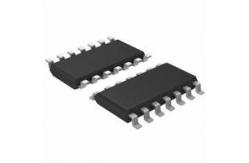
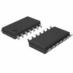
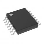
Fig.1 Pin configuration DIP14, SO14 and (T)SSOP14.
Fig.2 Pin configuration DHVQFN14.
Fig.3 Logic diagram (one gate).
Fig.4 Function diagram.
Fig.5 IEC logic symbol.