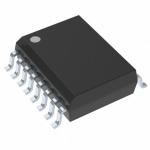
TLC2543CDWR Electronic IC Chips electronic device integrated circuit
|
|
Stock Offer (Hot Sell)
TLC2543C, TLC2543I, TLC2543M 12-BIT ANALOG-TO-DIGITAL CONVERTERS WITH SERIAL CONTROL AND 11 ANALOG INPUTS
description The TLC2543C and TLC2543I are 12-bit, switchedcapacitor, successive-approximation, analog-todigital converters. Each device, with three control inputs [chip select (CS), the input-output clock, and the address input (DATA INPUT)], is designed for communication with the serial port of a host processor or peripheral through a serial 3-state output. The device allows high-speed data transfers from the host.
In addition to the high-speed converter and versatile control capability, the device has an on-chip 14-channel multiplexer that can select any one of 11 inputs or any one of three internal self-test voltages. The sample-and-hold function is automatic. At the end of conversion, the end-of-conversion (EOC) output goes high to indicate that conversion is complete. The converter incorporated in the device features differential high-impedance reference inputs that facilitate ratiometric conversion, scaling, and isolation of analog circuitry from logic and supply noise. A switched-capacitor design allows low-error conversion over the full operating temperature range.
The TLC2543C is characterized for operation from TA = 0°C to 70°C. The TLC2543I is characterized for operation from TA = –40°C to 85°C. The TLC2543M is characterized for operation from TA = –55°C to 125°C.
absolute maximum ratings over operating free-air temperature range (unless otherwise noted)†
Supply voltage range, VCC (see Note 1) . . . . . . . . . . . . . . . . . . . . . . . . . . . . . . . . . . . . –0.5 V to 6.5 V Input voltage range, VI (any input) . . . . . . . . . . . . . . . . . . . . . . . . . . . . . . . . . . . –0.3 V to VCC + 0.3 V Output voltage range, VO . . . . . . . . . . . . . . . . . . . . . . . . . . . . . . . . . . . . . . . . . . –0.3 V to VCC + 0.3 V
Positive reference voltage, Vref+ . . . . . . . . . . . . . . . . . . . . . . . . . . . . . . . . . . . . . . . . . . . . VCC + 0.1 V Negative reference voltage, Vref– . . . . . . . . . . . . . . . . . . . . . . . . . . . . . . . . . . . . . . . . . . . . . . . . –0.1 V Peak input current, II (any input) . . . . . . . . . . . . . . . . . . . . . . . . . . . . . . . . . . . . . . . . . . . . . . . . ±20 mA Peak total input current, II (all inputs) . . . . . . . . . . . . . . . . . . . . . . . . . . . . . . . . . . . . . . . . . . . . . ±30 mA
Operating free-air temperature range, TA: TLC2543C . . . . . . . . . . . . . . . . . . . . . . . . . . . . 0°C to 70°C TLC2543I . . . . . . . . . . . . . . . . . . . . . . . . . . . . –40°C to 85°C TLC2543M . . . . . . . . . . . . . . . . . . . . . . . . . . –55°C to 125°C Storage temperature range, Tstg . . . . . . . . . . . . . . . . . . . . . . . . . . . . . . . . . . . . . . . . . . . –65°C to 150°C Lead temperature 1,6 mm (1/16 inch) from the case for 10 seconds . . . . . . . . . . . . . . . . . . . . . . . 260°C
† Stresses beyond those listed under “absolute maximum ratings” may cause permanent damage to the device. These are stress ratings only, and functional operation of the device at these or any other conditions beyond those indicated under “recommended operating conditions” is not implied. Exposure to absolute-maximum-rated conditions for extended periods may affect device reliability.
NOTE 1: All voltage values are with respect to the GND terminal with REF– and GND wired together (unless otherwise noted).
functional block diagram
|
|||||||||||||||||||||||||||||||||||||||||||||||||||||||||||||||||||||||||||||||||||||||||||||||||||||||||||||||||||||||||||||||||||||||||||||||||||||||||||
| Product Tags: electronic integrated circuit linear integrated circuits |