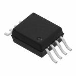
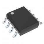
Original RT9173PS Electronic IC Chips Peak 3A Bus Termination Regulator
|
|
Stock Offer (Hot Sell)
RT9173/A Peak 3A Bus Termination Regulator
General Description The RT9173/A regulator is designed to convert voltage supplies ranging from 1.6V to 6V into a desired output voltage which adjusted by two external voltage divider resistors. The regulator is capable of sourcing or sinking up to 3A of peak current while regulating an output voltage to within 2% (DDR 1) and 3% (DDR 2) or less.
The RT9173/A, used in conjunction with series termination resistors, provides an excellent voltage source for active termination schemes of high speed transmission lines as those seen in high speed memory buses and distributed backplane designs. The voltage output of the regulator can be used as a termination voltage for DDR SDRAM.
Current limits in both sourcing and sinking mode, plus onchip thermal shutdown make the circuit tolerant of the output fault conditions.
Features
Applications
Absolute Maximum Ratings
Input Voltage ----------------------------------------------------------------------------------------------------- 7V Power Dissipation ----------------------------------------------------------------------------- Internally Limited ESD Rating ------------------------------------------------------------------------------------------------------ 2kV Storage Temperature Range ----------------------------------------------------------------- −65°C to 150°C Lead Temperature (Soldering, 10 sec.) ----------------------------------------------------------------- 260°C Power Dissipation, PD @ TA = 25°C TO-263-5-------------------------------------------------------------------------------------------------- 1.923W TO-252-5---------------------------------------------------------------------------------------------------1.471W SOP-8 ----------------------------------------------------------------------------------------------------- 0.625W Package Thermal Resistance (Note 1) TO-263-5, θJC ------------------------------------------------------------------------------------------- 7.7°C/W TO-252-5, θJC --------------------------------------------------------------------------------------------- 8°C/W SOP-8, θJC --------------------------------------------------------------------------------------------- 23.2°C /W TO-263-5,θJA --------------------------------------------------------------------------------------------- 52°C/W TO-252-5, θJA --------------------------------------------------------------------------------------------- 68°C/W SOP-8, θJA ------------------------------------------------------------------------------------------------ 160°C/W
Note 1. θJA is measured in the natural convection at TA = 25°C on a low effective thermal conductivity test board (single Layers, 1S) of JEDEC 51-3 thermal measurement standard. The case point of θJC is on the on the center of VCTRL pins (Lead 6 & 7) for SOP-8 packages, the center of heat sink (tab) for TO-252-5 and TO-263-5 packages.
Pin Configurations
Typical Application Circuit
Function Block Diagram
|
|||||||||||||||||||||||||||||||||||||||||||||||||||||||||||||||||||||||||||||||||||||||||||||||||||||||||||||||||||||||||||||||||||||||||||||||||||||||||||
| Product Tags: electronic integrated circuit linear integrated circuits |