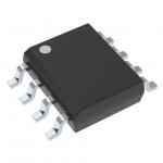
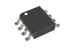
PIC12F675-I/SN Electronic IC Chips microchips and integrated circuits
|
|
Stock Offer (Hot Sell)
PIC12F629/675 8-Pin, Flash-Based 8-Bit CMOS Microcontrollers
High-Performance RISC CPU: • Only 35 Instructions to Learn - All single-cycle instructions except branches • Operating Speed: - DC – 20 MHz oscillator/clock input - DC – 200 ns instruction cycle
• Interrupt Capability • 8-Level Deep Hardware Stack • Direct, Indirect, and Relative Addressing modes
Special Microcontroller Features: • Internal and External Oscillator Options - Precision Internal 4 MHz oscillator factory calibrated to ±1% - External Oscillator support for crystals and resonators - 5 μs wake-up from Sleep, 3.0V, typical
• Power-Saving Sleep mode • Wide Operating Voltage Range – 2.0V to 5.5V • Industrial and Extended Temperature Range
• Low-Power Power-on Reset (POR) • Power-up Timer (PWRT) and Oscillator Start-up Timer (OST) • Brown-out Detect (BOD) • Watchdog Timer (WDT) with Independent Oscillator for Reliable Operation
• Multiplexed MCLR/Input Pin • Interrupt-on-Pin Change • Individual Programmable Weak Pull-ups • Programmable Code Protection
• High Endurance Flash/EEPROM Cell - 100,000 write Flash endurance - 1,000,000 write EEPROM endurance - Flash/Data EEPROM Retention: > 40 years
Low-Power Features: • Standby Current: - 1 nA @ 2.0V, typical • Operating Current: - 8.5 μA @ 32 kHz, 2.0V, typical - 100 μA @ 1 MHz, 2.0V, typical
• Watchdog Timer Current - 300 nA @ 2.0V, typical • Timer1 Oscillator Current: - 4 μA @ 32 kHz, 2.0V, typical
Peripheral Features: • 6 I/O Pins with Individual Direction Control • High Current Sink/Source for Direct LED Drive
• Analog Comparator module with: - One analog comparator - Programmable on-chip comparator voltage reference (CVREF) module - Programmable input multiplexing from device inputs - Comparator output is externally accessible
• Analog-to-Digital Converter module (PIC12F675): - 10-bit resolution - Programmable 4-channel input - Voltage reference input • Timer0: 8-Bit Timer/Counter with 8-Bit Programmable Prescaler
• Enhanced Timer1: - 16-bit timer/counter with prescaler - External Gate Input mode - Option to use OSC1 and OSC2 in LP mode as Timer1 oscillator, if INTOSC mode selected • In-Circuit Serial ProgrammiCM GROUPM (ICSPTM) via two pins
Absolute Maximum Ratings†
Ambient temperature under bias................................................................................... -40 to +125°C Storage temperature ................................................................................................ -65°C to +150°C Voltage on VDD with respect to VSS ............................................................................... -0.3 to +6.5V Voltage on MCLR with respect to Vss ............................................................................-0.3 to +13.5V Voltage on all other pins with respect to VSS .................................................... -0.3V to (VDD + 0.3V)
Total power dissipation(1) ........................................................................................................800 mW Maximum current out of VSS pin .............................................................................................. 300 mA Maximum current into VDD pin ................................................................................................. 250 mA Input clamp current, IIK (VI < 0 or VI > VDD)...............................................................................±20 mA Output clamp current, IOK (Vo < 0 or Vo >VDD) ........................................................................±20 mA
Maximum output current sunk by any I/O pin............................................................................... 25 mA Maximum output current sourced by any I/O pin ......................................................................... 25 mA Maximum current sunk by all GPIO ............................................................................................ 125 mA Maximum current sourced all GPIO ............................................................................................ 125 mA
Note 1: Power dissipation is calculated as follows: PDIS = VDD x {IDD - ∑ IOH} + ∑ {(VDD-VOH) x IOH} + ∑(VOl x IOL).
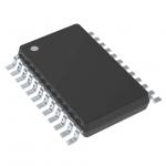
Pin Diagrams
|
|||||||||||||||||||||||||||||||||||||||||||||||||||||||||||||||||||||||||||||||||||||||||||||||||||||||||||||||||||||||||||||||||||||||||||||||||||||||||||
| Product Tags: digital integrated circuits linear integrated circuits |