
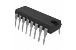
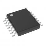
MC3487N Electronic IC Chips QUADRUPLE DIFFERENTIAL LINE DRIVER
|
|
Stock Offer (Hot Sell)
MC3487 QUADRUPLE DIFFERENTIAL LINE DRIVER
description The MC3487 offers four independent differential line drivers designed to meet the specifications of ANSI TIA/EIA-422-B and ITU Recommendation V.11. Each driver has a TTL-compatible input buffered to reduce current and minimize loading.
The driver outputs utilize 3-state circuitry to provide high-impedance states at any pair of differential outputs when the appropriate output enable is at a low logic level. Internal circuitry is provided to ensure the high-impedance state at the differential outputs during power-up and power-down transition times, provided the output enable is low.
The MC3487 is designed for optimum performance when used with the MC3486 quadruple line receiver. It is supplied in a 16-pin dual-in-line package and operates from a single 5-V supply.
absolute maximum ratings over operating free-air temperature range (unless otherwise noted)†
Supply voltage, VCC (see Note 1) . . . . . . . . . . . . . . . . . . . . . . . . . . . . . . . . . . . . . . . . . . . . . . . 8 V Input voltage, VI . . . . . . . . . . . . . . . . . . . . . . . . . . . . . . . . . . . . . . . . . . . . . . . . . . . . . . . . . . . 5.5 V Output voltage, VO . . . . . . . . . . . . . . . . . . . . . . . . . . . . . . . . . . . . . . . . . . . . . . . . . . . . . . . . . . 7 V Package thermal impedance, θJA (see Notes 2 and 3): D package . . . . . . . . . . . . . . . . . . 73°C/W N package . . . . . . . . . . . . . . . . . . 67°C/W NS package . . . . . . . . . . . . . . . . . 64°C/W Operating virtual junction temperature, TJ . . . . . . . . . . . . . . . . . . . . . . . . . . . . . . . . . . . . . . 150°C Storage temperature range, Tstg . . . . . . . . . . . . . . . . . . . . . . . . . . . . . . . . . . . . . −65 °C to 150°C
† Stresses beyond those listed under “absolute maximum ratings” may cause permanent damage to the device. These are stress ratings only, and functional operation of the device at these or any other conditions beyond those indicated under “recommended operating conditions” is not implied. Exposure to absolute-maximum-rated conditions for extended periods may affect device reliability. NOTES: 1. All voltage values, except differential output voltage, VOD, are with respect to the network ground terminal. 2. Maximum power dissipation is a function of TJ(max), θJA, and TA. The maximum allowable power dissipation at any allowable ambient temperature is PD = (TJ(max) − TA)/θJA. Operating at the absolute maximum TJ of 150°C can affect reliability. 3. The package thermal impedance is calculated in accordance with JESD 51-7.
recommended operating conditions
logic diagram (positive logic)
schematics of inputs and outputs
|
||||||||||||||||||||||||||||||||||||||||||||||||||||||||||||||||||||||||||||||||||||||||||||||||||||||||||||||||||||||||||||||||||||||||||||||||||||||||||||||||||||||||||||||||||||
| Product Tags: digital integrated circuits linear integrated circuits |
|
AD8552ARUZ Electronic IC Chip NEW AND ORIGINAL STOCK |
|
BA10358F-E2 Electronic IC Chip NEW AND ORIGINAL STOCK |
|
BA14741F-E2 Electronic IC Chip NEW AND ORIGINAL STOCK |
|
DRV602PWR Flash Memory IC NEW AND ORIGINAL STOCK |
|
OPA335AIDR Electronic IC Chips SINGLE-SUPPLY CMOS OPERATIONAL AMPLIFIERS |
|
OP90GSZ-REEL7 Electronic IC Chips Low-Voltage Operational Amplifier |