
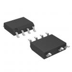
MAX890LESA Electronic IC Chips P-Channel Switch with Thermal Shutdown
|
|
Stock Offer (Hot Sell)
1.2A, Current-Limited, High-Side P-Channel Switch with Thermal Shutdown
General Description The MAX890L smart, low-voltage, P-channel, MOSFET power switch is intended for high-side load-switching applications. This switch operates with inputs from +2.7V to +5.5V, making it ideal for both +3V and +5V systems. Internal current-limiting circuitry protects the input supply against overload. Thermal-overload protection limits power dissipation and junction temperatures.
The MAX890L’s maximum current limit is 1.2A. The current limit through the switch is programmed with a resistor from SET to ground. The quiescent supply current is a low 10µA. When the switch is off, the supply current decreases to 0.1µA.
The MAX890L is available in an 8-pin SO package.
Applications PCMCIA Slots Access Bus Slots Portable Equipment
Features ♦ +2.7V to +5.5V Input Range ♦ Programmable Current Limit ♦ Low Quiescent Current 10µA (typ) at VIN = +3.3V 0.1µA (typ) with Switch Off ♦ Thermal Shutdown ♦ FAULT Indicator Output ♦ 0.09Ω (typ) On-Resistance
ABSOLUTE MAXIMUM RATINGS IN to GND ................................................................-0.3V to +6V ON, FAULT to GND .................................................-0.3V to +6V SET, OUT to GND ...................................... -0.3V to (VIN + 0.3V) Maximum Continuous Switch Current ..................................1.5A
Continuous Power Dissipation (TA = +70°C) SO (derate 5.88mW/°C above +70°C) ..........................471mW Operating Temperature Range MAX890LESA ....................................................-40°C to +85°C
Storage Temperature Range ........................... -65°C to +150°C Lead Temperature (soldering, 10s) . ...............................+300°C Soldering Temperature (reflow) .......................................+260°C
Stresses beyond those listed under “Absolute Maximum Ratings” may cause permanent damage to the device. These are stress ratings only, and functional operation of the device at these or any other conditions beyond those indicated in the operational sections of the specifications is not implied. Exposure to absolute maximum rating conditions for extended periods may affect device reliability.
Typical Operating Circuit
Pin Configuration
|
|||||||||||||||||||||||||||||||||||||||||||||||||||||||||||||||||||||||||||||||||||||||||||||||||||||||||||||||||||||||||||||||||||||||||||||||||||||||||||
| Product Tags: digital integrated circuits linear integrated circuits |
|
BTS724GXUMA1 Smart High-Side Power Switch Four Channels programmed integrated led circuit board |
|
TPS61041DBVR Electronic IC Chips LOW-POWER DC/DC BOOST CONVERTER |
|
US90AEVK Electronic IC Chips power ic chip 24V Hall IC Fan Driver |
|
TLE4226G Integrated Circuit Chip Intelligent Sixfold Low-Side Switch |
|
NCP1234AD65R2G Fixed Frequency Current Mode Controller for Flyback Converters |
|
REG1117FA-5.0 Integrated Circuit IC Chip Low Dropout Positive Regulator |