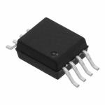
ADM202JRNZ Electronic IC Chips High Speed CMOS RS -232 Driver / Receivers
|
|
High-Speed, 5 V, 0.1 F CMOS RS-232 Driver/Receivers ADM202/ADM203
FEATURES
APPLICATIONS Computers Peripherals Modems Printers Instruments
GENERAL DESCRIPTION The ADM202/ADM203 is a two-channel RS-232 line driver/ receiver pair designed to operate from a single 5 V power supply. A highly efficient on-chip charge pump design permits RS-232 levels to be developed using charge pump capacitors as small as 0.1 µF. The capacitors are internal to the package on the ADM203 so no external capacitors are required. These converters generate ±10 V RS-232 output levels.
The ADM202/ADM203 meets or exceeds the EIA-232-E and V.28 specifications. Fast driver slew rates permit operation up to 120 kB while high-drive currents allow for extended cable leCM GROUPhs.
An epitaxial BiCMOS construction minimizes power consumption to 10 mW and also guards against latch-up. Overvoltage protection is provided allowing the receiver inputs to withstand continuous voltages in excess of ± 30 V. In addition, all pins contain ESD protection to levels greater than 2 kV.
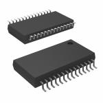
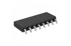
The ADM202 is available in 16-lead DIP and both narrow and wide SOIC packages. The ADM203 is available in a 20-lead DIP package.
ABSOLUTE MAXIMUM RATINGS* (TA = 25°C unless otherwise noted) VCC . . . . . . . . . . . . . . . . . . . . . . . . . . . . . . . . . . . . . . . . . . 6 V V+ . . . . . . . . . . . . . . . . . . . . . . . . . . . . (VCC – 0.3 V) to +14 V V– . . . . . . . . . . . . . . . . . . . . . . . . . . . . . . . . . +0.3 V to –14 V Input Voltages TIN . . . . . . . . . . . . . . . . . . . . . . . . . –0.3 V to (VCC + 0.3 V) RIN . . . . . . . . . . . . . . . . . . . . . . . . . . . . . . . . . . . . . . . ±30 V
Output Voltages TOUT . . . . . . . . . . . . . . . . . . . (V+, +0.3 V) to (V–, – 0.3 V) ROUT . . . . . . . . . . . . . . . . . . . . . . . –0.3 V to (VCC + 0.3 V) Short Circuit Duration TOUT . . . . . . . . . . . . . . . . . . . . . . . . . . . . . . . . . Continuous
Power Dissipation N-16 DIP . . . . . . . . . . . . . . . . . . . . . . . . . . . . . . . . 470 mW R-16N SOIC . . . . . . . . . . . . . . . . . . . . . . . . . . . . . 600 mW R-16W SOIC . . . . . . . . . . . . . . . . . . . . . . . . . . . . . 500 mW N-20 DIP . . . . . . . . . . . . . . . . . . . . . . . . . . . . . . . . 890 mW Thermal Impedance N-16 DIP . . . . . . . . . . . . . . . . . . . . . . . . . . . . . . . . 135°C/W R-16N SOIC . . . . . . . . . . . . . . . . . . . . . . . . . . . . . 105°C/W R-16W SOIC . . . . . . . . . . . . . . . . . . . . . . . . . . . . . 105°C/W N-20 DIP . . . . . . . . . . . . . . . . . . . . . . . . . . . . . . . . 125°C/W
Operating Temperature Range Commercial (J Version) . . . . . . . . . . . . . . . . . . 0°C to 70°C Storage Temperature Range . . . . . . . . . . . . –65°C to +150°C Lead Temperature Soldering Vapor Phase (60 sec) . . . . . . . . . . . . . . . . . . . . . . . . . 215°C Infrared (15 sec) . . . . . . . . . . . . . . . . . . . . . . . . . . . . . 220°C ESD Rating . . . . . . . . . . . . . . . . . . . . . . . . . . . . . . . . . . >2000 V
*This is a stress rating only and functional operation of the device at these or any other conditions above those indicated in the operation sections of this specification is not implied. Exposure to absolute maximum rating conditions for extended periods of time may affect reliability.
FUNCTIONAL BLOCK DIAGRAMS
Stock Offer (Hot Sell)
|
|||||||||||||||||||||||||||||||||||||||||||||||||||||||||||||||||||||||||||||||||||||||||||||||||||||||||||||||||||||||||||||||||||||||||||||||||||||||||||
| Product Tags: electronic integrated circuit linear integrated circuits |