
UCC2897A Electronic IC Chips microchips and integrated circuits
|
|
Stock Offer (Hot Sell)
UCC2897A ADVANCED CURRENT-MODE ACTIVE CLAMP PWM CONTROLLER
FEATURES
APPLICATIONS
DESCRIPTION The UCC2897A PWM controller simplifies implementation of the various active clamp/reset and synchronous rectifier switching power topologies.
The UCC2897A is a peak current-mode, fixedfrequency, high-performance pulse width modulator. It includes the logic and the drive capability for the P-channel auxiliary switch along with a simple method of programming the critical delays for proper active clamp operation.
Features include an internal programmable slope compensation circuit, precise DMAX limit, and a synchronizable oscillator with an internal timing capacitor. An accurate line monitoring function also programs the converter’s ON and OFF transitions with regard to the bulk input voltage, VIN.
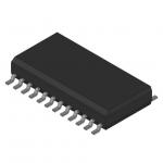
The UCC2897A adds a second level hiccup mode current sense threshold, bi-directional synchronization and input overvoltage protection functionalities. The UCC2897A is offered in 20-pin TSSOP (PW) and 20-pin QFN (RGP) package.
ABSOLUTE MAXIMUM RATINGS over operating free-air temperature range unless otherwise noted(1)
(1) Stresses beyond those listed under “absolute maximum ratings” may cause permanent damage to the device. These are stress ratings only, and functional operation of the device at these or any other conditions beyond those indicated under “recommended operating conditions” is not implied. Exposure to absolute-maximum-rated conditions for extended periods may affect device reliability. All voltages are with respect to GND. Currents are positive into and negative out of, the specified terminal.
TYPICAL APPLICATION DIAGRAM
|
|||||||||||||||||||||||||||||||||||||||||||||||||||||||||||||||||||||||||||||||||||||||||||||||||||||||||||||||||||||||||||||||||||||||||||||||||||||||||||||||||||||||||||||||||||||||||||||||
| Product Tags: electronic integrated circuit linear integrated circuits | |||||||||||||||||||||||||||||||||||||||||||||||||||||||||||||||||||||||||||||||||||||||||||||||||||||||||||||||||||||||||||||||||||||||||||||||||||||||||||||||||||||||||||||||||||||||||||||||
|
BTS724GXUMA1 Smart High-Side Power Switch Four Channels programmed integrated led circuit board |
|
TPS61041DBVR Electronic IC Chips LOW-POWER DC/DC BOOST CONVERTER |
|
US90AEVK Electronic IC Chips power ic chip 24V Hall IC Fan Driver |
|
TLE4226G Integrated Circuit Chip Intelligent Sixfold Low-Side Switch |
|
NCP1234AD65R2G Fixed Frequency Current Mode Controller for Flyback Converters |
|
REG1117FA-5.0 Integrated Circuit IC Chip Low Dropout Positive Regulator |