
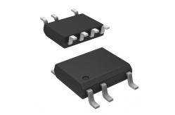
LNK606DG-TL Electronic IC Chip Energy - Efficient , Accurate CV / CC Switcher
|
|
LNK603-606/613-616 LinkSwitch-II Family Energy-Efficient, Accurate CV/CC Switcher for Adapters and Chargers
Product Highlights
Dramatically Simplifies CV/CC Converters • Eliminates optocoupler and all secondary CV/CC control circuitry • Eliminates all control loop compensation circuitry
Advanced Performance Features • Compensates for transformer inductance tolerances • Compensates for input line voltage variations • Compensates for cable voltage drop (LNK61X series) • Compensates for external component temperature variations • Very tight IC parameter tolerances using proprietary trimming technology • Frequency jittering greatly reduces EMI filter cost • Even tighter output tolerances achievable with external resistor selection/trimming • Programmable switching frequency up to 85 kHz to reduce transformer size
Advanced Protection/Safety Features • Auto-restart protection reduces power delivered by >95% for output short circuit and control loop faults (open and shorted components) • Hysteretic thermal shutdown – automatic recovery reduces power supply returns from the field • Meets high voltage creepage requirements between DRAIN and all other pins both on the PCB and at the package
EcoSmart® – Energy Efficient • Easily meets all global energy efficiency regulations • No-load consumption below 30 mW at 230 VAC with optional external bias winding • ON/OFF control provides constant efficiency down to very light loads – ideal for CEC and ENERGY STAR 2.0 regulations • No current sense resistors – maximizes efficiency
Green Package • Halogen free and RoHS compliant package
Applications • Chargers for cell/cordless phones, PDAs, MP3/portable audio devices, adapters, LED drivers, etc.
Description The LinkSwitch-II dramatically simplifies low power CV/CC charger designs by eliminating an optocoupler and secondary control circuitry. The device introduces a revolutionary control technique to provide very tight output voltage and current regulation, compensating for transformer and internal parameter tolerances along with input voltage variations.
The device incorporates a 700 V power MOSFET, a novel ON/OFF control state machine, a high voltage switched current source for self biasing, frequency jittering, cycle-by-cycle current limit and hysteretic thermal shutdown circuitry onto a monolithic IC.
Absolute Maximum Ratings(1,4) DRAIN Voltage .........................................................-0.3 V to 700 V DRAIN Peak Current: LNK603/613...................320 (480) mA(4) LNK604/614 .................. 400 (600) mA(4) LNK605/615 .................. 504 (750) mA(4) LNK606/616.................. 654 (980) mA(4) Peak Negative Pulsed Drain Current ............................ -100 mA(2) FEEDBACK Pin Voltage ............................................... -0.3 V to 9 V FEEDBACK Pin Current ...................................................... 100 mA BYPASS Pin Voltage ..................................... ............. -0.3 V to 9 V Storage Temperature ........................................... -65 °C to 150 °C Operating Junction Temperature ......................... -40 °C to 150 °C Lead Temperature(3) .......................................................... 260 °C Notes: 1. All voltages referenced to SOURCE, TA = 25 °C. 2. Duration not to exceed 2 msec. 3. 1/16 in. from case for 5 seconds. 4. The higher peak DRAIN current is allowed while the DRAIN voltage is simultaneously less than 400 V. 5. Maximum ratings specified may be applied, one at a time without causing permanent damage to the product. Exposure to Absolute Maximum ratings for extended periods of time may affect product reliability.
Stock Offer (Hot Sell)
|
|||||||||||||||||||||||||||||||||||||||||||||||||||||||||||||||||||||||||||||||||||||||||||||||||||||||||||||||||||||||||||||||||||||||||||||||||||||||||||
| Product Tags: electronic integrated circuit linear integrated circuits |
|
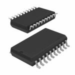
BTS724GXUMA1 Smart High-Side Power Switch Four Channels programmed integrated led circuit board |
|
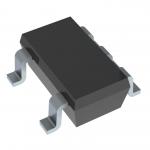
TPS61041DBVR Electronic IC Chips LOW-POWER DC/DC BOOST CONVERTER |
|
US90AEVK Electronic IC Chips power ic chip 24V Hall IC Fan Driver |
|
TLE4226G Integrated Circuit Chip Intelligent Sixfold Low-Side Switch |
|
NCP1234AD65R2G Fixed Frequency Current Mode Controller for Flyback Converters |
|
REG1117FA-5.0 Integrated Circuit IC Chip Low Dropout Positive Regulator |