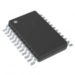
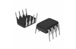
TL072CP Electronic IC Chips LOW-NOISE JFET-INPUT OPERATIONAL AMPLIFIERS
|
|
TL071, TL071A, TL071B, TL072 TL072A, TL072B, TL074, TL074A, TL074B LOW-NOISE JFET-INPUT OPERATIONAL AMPLIFIERS
• Low Power Consumption • Wide Common-Mode and Differential Voltage Ranges • Low Input Bias and Offset Currents • Output Short-Circuit Protection • Low Total Harmonic Distortion . . . 0.003% Typ
• Low Noise Vn = 18 nV/√Hz Typ at f = 1 kHz • High Input Impedance . . . JFET Input Stage • Internal Frequency Compensation • Latch-Up-Free Operation • High Slew Rate . . . 13 V/μs Typ • Common-Mode Input Voltage Range Includes VCC+ des
description The JFET-input operational amplifiers in the TL07x series are similar to the TL08x series, with low input bias and offset currents and fast slew rate. The low harmonic distortion and low noise make the TL07x series ideally suited for high-fidelity and audio preamplifier applications. Each amplifier features JFET inputs (for high input impedance) coupled with bipolar output stages integrated on a single monolithic chip.
The C-suffix devices are characterized for operation from 0°C to 70°C. The I-suffix devices are characterized for operation from −40°C to 85°C. The M-suffix devices are characterized for operation over the full military temperature range of −55°C to 125°C.
absolute maximum ratings over operating free-air temperature range (unless otherwise noted)† Supply voltage (see Note 1): VCC+ . . . . . . . . . . . . . . . . . . . . . . . . . . . . . . . . . . . . . . . . . . . 18 V VCC− . . . . . . . . . . . . . . . . . . . . . . . . . . . . . . . . . . . . . . . . . . −18 V Differential input voltage, VID (see Note 2) . . . . . . . . . . . . . . . . . . . . . . . . . . . . . . . . . . . . . ±30 V Input voltage, VI (see Notes 1 and 3) . . . . . . . . . . . . . . . . . . . . . . . . . . . . . . . . . . . . . . . . . ±15 V Duration of output short circuit (see Note 4) . . . . . . . . . . . . . . . . . . . . . . . . . . . . . . . . . Unlimited Package thermal impedance, θJA (see Notes 5 and 6): D package (8 pin) . . . . . . . . . . . 97°C/W D package (14 pin) . . . . . . . . . . 86°C/W N package . . . . . . . . . . . . . . . . . 80°C/W NS package . . . . . . . . . . . . . . . 76°C/W P package . . . . . . . . . . . . . . . . . 85°C/W PS package . . . . . . . . . . . . . . . . 95°C/W PW package (8 pin) . . . . . . . . . 149°C/W PW package (14 pin) . . . . . . . . 113°C/W U package . . . . . . . . . . . . . . . . 185°C/W Package thermal impedance, θJC (see Notes 7 and 8): FK package . . . . . . . . . . . . . . 5.61°C/W J package . . . . . . . . . . . . . . . 15.05°C/W JG package . . . . . . . . . . . . . . . 14.5°C/W W package . . . . . . . . . . . . . . . 14.65°C/W Operating virtual junction temperature, TJ . . . . . . . . . . . . . . . . . . . . . . . . . . . . . . . . . . . . . . 150°C Case temperature for 60 seconds: FK package . . . . . . . . . . . . . . . . . . . . . . . . . . . . . . . . . . 260°C Lead temperature 1,6 mm (1/16 inch) from case for 10 seconds: J, JG, or W package . . . . . 300°C Storage temperature range, Tstg . . . . . . . . . . . . . . . . . . . . . . . . . . . . . . . . . . . . . . . −65°C to 150°C †Stresses beyond those listed under “absolute maximum ratings” may cause permanent damage to the device. These are stress ratings only, and functional operation of the device at these or any other conditions beyond those indicated under “recommended operating conditions” is not implied. Exposure to absolute-maximum-rated conditions for extended periods may affect device reliability. NOTES: 1. All voltage values, except differential voltages, are with respect to the midpoint between VCC+ and VCC−. 2. Differential voltages are at IN+, with respect to IN−. 3. The magnitude of the input voltage must never exceed the magnitude of the supply voltage or 15 V, whichever is less. 4. The output may be shorted to ground or to either supply. Temperature and/or supply voltages must be limited to ensure that the dissipation rating is not exceeded. 5. Maximum power dissipation is a function of TJ(max), θJA, and TA. The maximum allowable power dissipation at any allowable ambient temperature is PD = (TJ(max) − TA)/θJA. Operating at the absolute maximum TJ of 150°C can affect reliability. 6. The package thermal impedance is calculated in accordance with JESD 51-7. 7. Maximum power dissipation is a function of TJ(max), θJC, and TC. The maximum allowable power dissipation at any allowable case temperature is PD = (TJ(max) − TC)/θJC. Operating at the absolute maximum TJ of 150°C can affect reliability. 8. The package thermal impedance is calculated in accordance with MIL-STD-883.
symbols
Stock Offer (Hot Sell)
|
|||||||||||||||||||||||||||||||||||||||||||||||||||||||||||||||||||||||||||||||||||||||||||||||||||||||||||||||||||||||||||||||||||||||||||||||||||||||||||
| Product Tags: electronic integrated circuit linear integrated circuits |