LT1763CS8#TRPBF Electronic IC Chips Low Noise , LDO Micropower Regulators
|
|
LT1763 Series 500mA, Low Noise, LDO Micropower Regulators
FEATURES ■ Low Noise: 20µVRMS (10Hz to 100kHz) ■ Output Current: 500mA ■ Low Quiescent Current: 30µA ■ Wide Input Voltage Range: 1.8V to 20V ■ Low Dropout Voltage: 300mV ■ Very Low Shutdown Current: < 1µA ■ No Protection Diodes Needed ■ Fixed Output Voltages: 1.5V, 1.8V, 2.5V, 3V, 3.3V, 5V
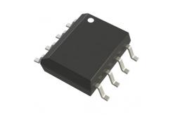
■ Adjustable Output from 1.22V to 20V ■ Stable with 3.3µF Output Capacitor ■ Stable with Aluminum, Tantalum or Ceramic Capacitors ■ Reverse Battery Protection ■ No Reverse Current ■ Overcurrent and Overtemperature Protected ■ 8-Lead SO Package
APPLICATIONS ■ Cellular Phones ■ Battery-Powered Systems ■ Noise-Sensitive Instrumentation Systems
DESCRIPTION The LT® 1763 series are micropower, low noise, low dropout regulators. The devices are capable of supplying 500mA of output current with a dropout voltage of 300mV. Designed for use in battery-powered systems, the low 30µA quiescent current makes them an ideal choice. Quiescent current is well controlled; it does not rise in dropout as it does with many other regulators.
A key feature of the LT1763 regulators is low output noise. With the addition of an external 0.01µF bypass capacitor, output noise drops to 20µVRMS over a 10Hz to 100kHz bandwidth. The LT1763 regulators are stable with output capacitors as low as 3.3µF. Small ceramic capacitors can be used without the series resistance required by other regulators.
Internal protection circuitry includes reverse battery protection, current limiting, thermal limiting and reverse current protection. The parts come in fixed output voltages of 1.5V, 1.8V, 2.5V, 3V, 3.3V and 5V, and as an adjustable device with a 1.22V reference voltage. The LT1763 regulators are available in the 8-lead SO package.
TYPICAL APPLICATION
ABSOLUTE MAXIMUM RATINGS (Note 1)
IN Pin Voltage ........................................................ ±20V OUT Pin Voltage .................................................... ±20V Input to Output Differential Voltage ....................... ±20V SENSE Pin Voltage ............................................... ±20V ADJ Pin Voltage ...................................................... ±7V BYP Pin Voltage.................................................... ±0.6V SHDN Pin Voltage ................................................. ±20V Output Short-Circut Duration .......................... Indefinite Operating Junction Temperature Range (Note 2) ............................................ –40°C to 125°C Storage Temperature Range ................. –65°C to 150°C Lead Temperature (Soldering, 10 sec).................. 300°C Note 1: Absolute Maximum Ratings are those values beyond which the life of a device may be impaired.
Stock Offer (Hot Sell)
|
|||||||||||||||||||||||||||||||||||||||||||||||||||||||||||||||||||||||||||||||||||||||||||||||||||||||||||||||||||||||||||||||||||||||||||||||||||||||||||
| Product Tags: electronic integrated circuit linear integrated circuits |