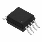
LM311P electronic integrated circuit DIFFERENTIAL COMPARATORS WITH STROBES
|
|
LM111, LM211, LM311 DIFFERENTIAL COMPARATORS WITH STROBES
• Fast Response Times • Strobe Capability • Maximum Input Bias Current . . . 300 nA • Maximum Input Offset Current . . . 70 nA • Can Operate From Single 5-V Supply • Available in Q-Temp Automotive − High-Reliability Automotive Applications − Configuration Control/Print Support − Qualification to Automotive Standards
description The LM111, LM211, and LM311 are single high-speed voltage comparators. These devices are designed to operate from a wide range of power-supply voltages, including ±15-V supplies for operational amplifiers and 5-V supplies for logic systems. The output levels are compatible with most TTL and MOS circuits. These comparators are capable of driving lamps or relays and switching voltages up to 50 V at 50 mA. All inputs and outputs can be isolated from system ground. The outputs can drive loads referenced to ground, VCC+ or VCC−. Offset balancing and strobe capabilities are available, and the outputs can be wire-OR connected. If the strobe is low, the output is in the off state, regardless of the differential input.
functional block diagram
absolute maximum ratings over operating free-air temperature range (unless otherwise noted)† Supply voltage: VCC+ (see Note 1) . . . . . . . . . . . . . . . . . . . . . . . . . . . . . . . . . . . . . . 18 V VCC− (see Note 1) . . . . . . . . . . . . . . . . . . . . . . . . . . . . . . . . . . . . . . −18 V VCC+ − VCC− . . . . . . . . . . . . . . . . . . . . . . . . . . . . . . . . . . . . . . . . . . . 36 V Differential input voltage, VID (see Note 2) . . . . . . . . . . . . . . . . . . . . . . . . . . . . . . . . ±30 V Input voltage, VI (either input, see Notes 1 and 3) . . . . . . . . . . . . . . . . . . . . . . . . . . ±15 V Voltage from emitter output to VCC− . . . . . . . . . . . . . . . . . . . . . . . . . . . . . . . . . . . . . 30 V Voltage from collector output to VCC−: LM111 . . . . . . . . . . . . . . . . . . . . . . . . . . . . . . 50 V LM211 . . . . . . . . . . . . . . . . . . . . . . . . . . . . . . 50 V LM211Q . . . . . . . . . . . . . . . . . . . . . . . . . . . . . 50 V LM311 . . . . . . . . . . . . . . . . . . . . . . . . . . . . . . 40 V Duration of output short circuit (see Note 4) . . . . . . . . . . . . . . . . . . . . . . . . . . . . . . . . 10 s Package thermal impedance, θJA (see Notes 5 and 6): D package . . . . . . . . . . . . . . 97°C/W P package . . . . . . . . . . . . . . . 85°C/W PS package . . . . . . . . . . . . . . 95°C/W PW package . . . . . . . . . . . . . .149°C/W Package thermal impedance, θJC (see Notes 7 and 8): FK package . . . . . . . . . . . . . . 5.61°C/W JG package . . . . . . . . . . . . . . .14.5°C/W Operating virtual junction temperature, TJ . . . . . . . . . . . . . . . . . . . . . . . . . . . . . . . . . . . . . . . . . 150°C Case temperature for 60 seconds: FK package . . . . . . . . . . . . . . . . . . . . . . . . . . . . . . . . . . . . . 260°C Lead temperature 1,6 mm (1/16 inch) from case for 10 seconds: J or JG package . . . . . . . . . . 300°C Lead temperature 1,6 mm (1/16 inch) from case for 60 seconds: D, P, PS, or PW package . . . . 260°C Storage temperature range, Tstg . . . . . . . . . . . . . . . . . . . . . . . . . . . . . . . . . . . . . . . . −65°C to 150°C † Stresses beyond those listed under “absolute maximum ratings” may cause permanent damage to the device. These are stress ratings only, and functional operation of the device at these or any other conditions beyond those indicated under “recommended operating conditions” is not implied. Exposure to absolute-maximum-rated conditions for extended periods may affect device reliability. NOTES: 1. All voltage values, unless otherwise noted, are with respect to the midpoint between VCC+ and VCC−. 2. Differential voltages are at IN+ with respect to IN−. 3. The magnitude of the input voltage must never exceed the magnitude of the supply voltage or ±15 V, whichever is less. 4. The output may be shorted to ground or either power supply. 5. Maximum power dissipation is a function of TJ(max), θJA, and TA. The maximum allowable power dissipation at any allowable ambient temperature is PD = (TJ(max) − TA)/θJA. Operating at the absolute maximum TJ of 150°C can affect reliability. 6. The package thermal impedance is calculated in accordance with JESD 51-7. 7. Maximum power dissipation is a function of TJ(max), θJC, and TC. The maximum allowable power dissipation at any allowable case temperature is PD = (TJ(max) − TC)/θJC. Operating at the absolute maximum TJ of 150°C can affect reliability. 8. The package thermal impedance is calculated in accordance with MIL-STD-883.
Stock Offer (Hot Sell)
|
|||||||||||||||||||||||||||||||||||||||||||||||||||||||||||||||||||||||||||||||||||||||||||||||||||||||||||||||||||||||||||||||||||||||||||||||||||||||||||
| Product Tags: electronic integrated circuit linear integrated circuits |