
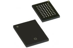
CY62157EV30LL-45BVXI Electronic IC Chips 8-Mbit (512K x 16) Static RAM
|
|
CY62157EV30 MoBL® 8-Mbit (512K x 16) Static RAM
Features • TSOP I package configurable as 512K x 16 or as 1M x 8 SRAM • High speed: 45 ns • Wide voltage range: 2.20V–3.60V • Pin compatible with CY62157DV30 • Ultra low standby power — Typical Standby current: 2 µA — Maximum Standby current: 8 µA (Industrial)
• Ultra low active power — Typical active current: 1.8 mA @ f = 1 MHz • Easy memory expansion with CE1, CE2, and OE features • Automatic power down when deselected • CMOS for optimum speed and power • Available in both Pb-free and non Pb-free 48-ball VFBGA, Pb-free 44-pin TSOP II and 48-pin TSOP I packages
Functional Description[1] The CY62157EV30 is a high performance CMOS static RAM organized as 512K words by 16 bits. This device features advanced circuit design to provide ultra low active current. This is ideal for providing More Battery Life™ (MoBL®) in portable applications such as cellular telephones. The device also has an automatic power down feature that significantly reduces power consumption when addresses are not toggling. Place the device into standby mode when deselected (CE1 HIGH or CE2 LOW or both BHE and BLE are HIGH). The input or output pins (IO0 through IO15) are placed in a high impedance state when:
• Deselected (CE1HIGH or CE2 LOW) • Outputs are disabled (OE HIGH) • Both Byte High Enable and Byte Low Enable are disabled (BHE, BLE HIGH) • Write operation is active (CE1 LOW, CE2 HIGH and WE LOW)
To write to the device, take Chip Enable (CE1 LOW and CE2 HIGH) and Write Enable (WE) inputs LOW. If Byte Low Enable (BLE) is LOW, then data from IO pins (IO0 through IO7) is written into the location specified on the address pins (A0 through A18). If Byte High Enable (BHE) is LOW, then data from IO pins (IO8 through IO15) is written into the location specified on the address pins (A0 through A18).
To read from the device, take Chip Enable (CE1 LOW and CE2 HIGH) and Output Enable (OE) LOW while forcing the Write Enable (WE) HIGH. If Byte Low Enable (BLE) is LOW, then data from the memory location specified by the address pins appear on IO0 to IO7. If Byte High Enable (BHE) is LOW, then data from memory appears on IO8 to IO15.
Logic Block Diagram
Notes 1. For best practice recommendations, please refer to the Cypress application note AN1064, SRAM System Guidelines
Maximum Ratings Exceeding maximum ratings may shorten the battery life of the device. User guidelines are not tested.
Storage Temperature .........................................................................–65°C to + 150°C Ambient Temperature with Power Applied ...........................................–55°C to + 125°C Supply Voltage to Ground Potential ................................–0.3V to 3.9V (VCCmax + 0.3V) DC Voltage Applied to Outputs in High-Z State [6, 7].........–0.3V to 3.9V (VCCmax + 0.3V) DC Input Voltage [6, 7] .................................................... –0.3V to 3.9V (VCC max + 0.3V) Output Current into Outputs (LOW) ....................................................................... 20 mA Static Discharge Voltage ....................................... > 2001V (MIL-STD-883, Method 3015) Latch up Current ............................................................................................... > 200 mA
Stock Offer (Hot Sell)
|
|||||||||||||||||||||||||||||||||||||||||||||||||||||||||||||||||||||||||||||||||||||||||||||||||||||||||||||||||||||||||||||||||||||||||||||||||||||||||||
| Product Tags: electronic integrated circuit linear integrated circuits |
|
SST26VF032B-104I/MF FLASH Memory IC 32Mbit SPI - Quad I/O 104 MHz 8-WDFN (5x6) |

|
SST26VF032B-104I/MF Flash Memory Chip IC Micro 32 Mbit Low Power Consumption |
|
LPC1768FBD100K MCU Chips IC MCU 32BIT 512KB FLASH 100LQFP 32 BIT Micro Controllers |

|
EPCS16SI8N NEW AND ORIGINAL STOCK |
|
Professional Flash Memory Products Ic Memory Chip XCF08PVOG48C |

|
M45PE10-VMN6P Flash Memory IC NEW AND ORIGINAL STOCK |