
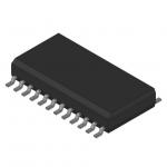
0.5a High-Side Driver Integrated Circuit Chip Industrial Intelligent Power Switch TDE1898RDP
|
|
TDE1897R TDE1898R 0.5A HIGH-SIDE DRIVER INDUSTRIAL INTELLIGENT POWER SWITCH
*0.5A OUTPUT CURRENT MULTIPOWER BCD TECHNOLOGY *18V TO 35V SUPPLY VOLTAGE RANGE *INTERNAL CURRENT LIMITING *THERMAL SHUTDOWN *OPEN GROUND PROTECTION *INTERNAL NEGATIVE VOLTAGE CLAMPING TO VS - 45V FOR FAST DEMAGNETIZATION *DIFFERENTIAL INPUTS WITH LARGE COM- MON MODE RANGE AND THRESHOLD HYSTERESIS *UNDERVOLTAGELOCKOUTWITH HYSTERESIS *OPEN LOAD DETECTION *TWO DIAGNOSTIC OUTPUTS *OUTPUT STATUS LED DRIVER
DESCRIPTION The TDE1897R/TDE1898R is a monolithic Intelligent Power Switch in Multipower BCD Technology, for driving inductive or resistive loads. An internal Clamping Diode enables the fast demagnetization of inductive loads. Diagnostic for CPU feedback and extensive use of electrical protections make this device inherently indistructible and suitable for general purpose industrial applications.
BLOCK DIAGRAM
PIN CONNECTIONS (Top view)
ABSOLUTE MAXIMUM RATINGS (Minidip pin reference)
THERMAL DATA
|
|||||||||||||||||||||||||||||||||||||||||||||||||||||||||||||||||
| Product Tags: small scale integrated circuits integrated components | |||||||||||||||||||||||||||||||||||||||||||||||||||||||||||||||||
|
BTS724GXUMA1 Smart High-Side Power Switch Four Channels programmed integrated led circuit board |
|
TPS61041DBVR Electronic IC Chips LOW-POWER DC/DC BOOST CONVERTER |
|
US90AEVK Electronic IC Chips power ic chip 24V Hall IC Fan Driver |
|
TLE4226G Integrated Circuit Chip Intelligent Sixfold Low-Side Switch |
|
NCP1234AD65R2G Fixed Frequency Current Mode Controller for Flyback Converters |
|
REG1117FA-5.0 Integrated Circuit IC Chip Low Dropout Positive Regulator |