
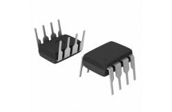
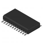
Current Mode Pwm Controller UC3844AM Integrated Circuit Components
|
|
CURRENT MODE PWM CONTROLLER
DESCRIPTION The UC184xA family of control ICs provides all the necessary features to implement off-line fixed-frequency, current-mode switching power supplies with a minimum of external components. The current mode architecture demonstrates improved load regulation, pulse-by-pulse current limiting and inherent protection of the power supply output switch. The IC includes: A bandgap reference trimmed to ±1% accuracy, an error amplifier, a current sense comparator with internal clamp to 1V, a high current totem pole output stage for fast switching of power MOSFET's, and an externally programmable oscillator to set frequency and maximum duty cycle. The undervoltage lock-out is designed to operate with 250µA typ. start-up current, allowing an efficient bootstrap supply voltage design. Available options for this family of products, such as start-up voltage hysteresis and duty cycle, are summarized below in the Available Options section. The UC184xA family of control ICs is also available in 14-pin SOIC package which makes the Power Output Stage Collector and Ground pins available.
PRODUCT HIGHLIGHT
KEY FEATURES
APPLICATIONS ■ ECONOMICAL OFF-LINE FLYBACK OR FORWARD CONVERTERS. ■ DC-DC BUCK OR BOOST CONVERTERS. ■ LOW COST DC MOTOR CONTROL.
ABSOLUTE MAX IMUM RAT INGS (Note 1) Supply Voltage (Low Impedance Source) (VCC) ......................................................... 30V Supply Voltage (ICC < 30mA).......................................................................... Self Limiting Output Current ............................................................................................................. ±1A Output Energy (Capacitive Load)................................................................................. 5µJ Analog Inputs (VFB & ISENSE) ........................................................................ -0.3V to +6.3V Error Amp Output Sink Current ............................................................................... 10mA Power Dissipation at TA = 25°C (M Package) .............................................................. 1W Storage Temperature Range .................................................................... -65°C to +150°C Lead Temperature (Soldering, 10 Seconds) ............................................................. 300°C
Note 1. Exceeding these ratings could cause damage to the device. All voltages are with respect to Ground. Currents are positive into, negative out of the specified terminal. Pin numbers refer to DIL packages only.
PACKAGE PIN OUTS THERMAL DATA
Junction Temperature Calculation: TJ = TA + (PD x θJA). The θJA numbers are guidelines for the thermal performance of the device/pc-board system. All of the above assume no ambient airflow |
||||||||
| Product Tags: chip in electronics small scale integrated circuits |
|
BTS724GXUMA1 Smart High-Side Power Switch Four Channels programmed integrated led circuit board |
|
TPS61041DBVR Electronic IC Chips LOW-POWER DC/DC BOOST CONVERTER |
|
US90AEVK Electronic IC Chips power ic chip 24V Hall IC Fan Driver |
|
TLE4226G Integrated Circuit Chip Intelligent Sixfold Low-Side Switch |
|
NCP1234AD65R2G Fixed Frequency Current Mode Controller for Flyback Converters |
|
REG1117FA-5.0 Integrated Circuit IC Chip Low Dropout Positive Regulator |