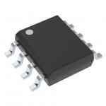
Integrated Components UPC339C Low Power Quad Comparator Common Mode Input
|
|
Integrated Components UPC339C Low Power Quad Comparator Common Mode Input
LOW POWER QUAD COMPARATOR DESCRIPTION The µPC339 is a quad comparator which is designed to operate from a single power supply over a wide range of voltage. Operation from split power supplies, is also possible and the power supply current drain is very low. Further advantage, the input common-mode voltage includes ground, even though operated from a single power supply voltage.
FEATURES • Common-mode input voltage range includes V– • Wide supply voltage range 2 V to 32 V (Single) ±1 V to ±16 V (Split) • Low supply current • Open collector output
EQUIVALENT CIRCUIT (1/4 Circuit) PIN CONFIGURATION (Top View)
Notes 1. Reverse connection of supply voltage can cause destruction. 2. The input voltage should be allowed to input without damage or destruction independent of the magnitude of V+. Either input signal should not be allowed to go negative by more than 0.3 V. The normal operation will establish when any input is within the Common Mode Input Voltage Range of electrical characteristics. 3. This specification is the voltage which should be allowed to supply to the output terminal from external without damage or destruction independent of the magnitude of V+. Even during the transition period of supply voltage, power on/off etc., this specification should be kept. 4. Thermal derating factor is –7.6 mW/°C when operating ambient temperature is higher than 55 °C. 5. Thermal derating factor is –5.5 mW/°C when operating ambient temperature is higher than 25 °C. 6. Short circuits from the output to V+ can cause destruction. Pay careful attention to the total power dissipation not to exceed the absolute maximum ratings, Note 4 and Note 5.
APPLICATION CIRCUIT EXAMPLE
|
||||||||||||||||||||||||||||||||||||||
| Product Tags: small scale integrated circuits integrated components |