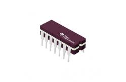
Microchips And Integrated Circuits SN74HC132N Schmitt Trigger Inputs
|
|
Microchips And Integrated Circuits SN74HC132N Schmitt Trigger Inputs
Features Wide Operating Voltage Range of 2 V to 6 V Outputs Can Drive Up To 10 LSTTL Loads Low Power Consumption, 20-µA Max ICC Typical tpd = 14 ns ±4-mA Output Drive at 5 V Low Input Current of 1 µA Max Operation From Very Slow Input Transitions Temperature-Compensated Threshold Levels High Noise Immunity Same Pinouts as ’HC00
description/ordering information Each circuit functions as a NAND gate, but because of the Schmitt action, it has different input threshold levels for positive- and negative-going signals. The ’HC132 devices perform the Boolean function Y = A • B or Y = A + B in positive logic. These circuits are temperature compensated and can be triggered from the slowest of input ramps and still give clean jitter-free output signals.
absolute maximum ratings over operating free-air temperature range (unless otherwise noted)†
Supply voltage range, VCC −0.5 V to 7 V Input clamp current, IIK (VI < 0 or VI > VCC) (see Note 1) ±20 mA Output clamp current, IOK (VO < 0 or VO > VCC) (see Note 1) ±20 mA Continuous output current, IO (VO = 0 to VCC) . ±25 mA Continuous current through VCC or GND . ±50 mA Package thermal impedance, θJA (see Note 2): D package 86 . . . . . . . . . . . . . . . . . . . . . . . . . . . . . . . . . . . °C/W DB package 96 . . . . . . . . . . . . . . . . . . . . . . . . . . . . . . . . . °C/W N package 80 . . . . . . . . . . . . . . . . . . . . . . . . . . . . . . . . . . . °C/W NS package 76 . . . . . . . . . . . . . . . . . . . . . . . . . . . . . . . . . °C/W PW package 113 . . . . . . . . . . . . . . . . . . . . . . . . . . . . . . . . °C/W
† Stresses beyond those listed under “absolute maximum ratings” may cause permanent damage to the device. These are stress ratings only, and functional operation of the device at these or any other conditions beyond those indicated under “recommended operating conditions” is not implied. Exposure to absolute-maximum-rated conditions for extended periods may affect device reliability. NOTES: 1. The input and output voltage ratings may be exceeded if the input and output current ratings are observed. 2. The package thermal impedance is calculated in accordance with JESD 51-7.
PARAMETER MEASUREMENT INFORMATION
|
|||||||||||||||||||||||||||||||||||||||||||||||
| Product Tags: chip in electronics integrated components | |||||||||||||||||||||||||||||||||||||||||||||||