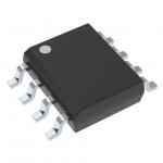
Optical Integrated Circuit Chip High Precision Dual Operational Amplifiers TLC27L2C
|
|
Optical Integrated Circuit Chip High Precision Dual Operational Amplifiers
TLC27L2C PLincmose Precision Dual Operational Amplifiers ESD-Protection Circuitry
Trimmed Offset Voltage: TLC27L7 . . . 500 µV Max at 25°C, VDD = 5 V Input Offset Voltage Drift . . . Typically 0.1 µV/Month, including the First 30 Days
Wide Range of Supply Voltages Over Specified Temperature Range: 0°C to 70°C . . . 3 V to 16 V –40°C to 85°C . . . 4 V to 16 V –55°C to 125°C . . . 4 V to 16 V
Single-Supply Operation
Common-Mode Input Voltage Range Extends Below the Negative Rail (C-Suffix, I-Suffix Types)
Ultra-Low Power...Typically 95 µW at 25°C, VDD = 5 V
Output Voltage Range includes Negative Rail
High Input Impedance . . . 1012 Ω Typ
ESD-Protection Circuitry Small-Outline Package Option Also Available in Tape and Reel Designed-In Latch-Up immunity
description
The TLC27L2 and TLC27L7 dual operational amplifiers
combine a wide range of input offset voltage grades with low
offset voltage drift, high input impedance, extremely low
power, and high gain.
These devices use Texas Instruments silicon-gate LinCMOS technology, which provides offset voltage stability far exceeding the stability available with conventional metal-gate processes.
The extremely high input impedance, low bias currents, and low power consumption make these cost-effective devices ideal for high gain, low frequency, low power applications. Four offset voltage grades are available (C-suffix and I-suffix types), ranging from the low-cost TLC27L2 (10 mV) to the high-precision TLC27L7 (500 µV). These advantages, in combination with good common-mode rejection and supply voltage rejection, make these devices a good choice for new state-of-the-art designs as well as for upgrading existing designs.
In general, many features associated with bipolar technology are available in LinCMOS operational amplifiers, without the power penalties of bipolar technology. General applications such as transducer interfacing, analog calculations, amplifier blocks, active filters, and signal buffering are easily designed with the TLC27L2 and TLC27L7. The devices also exhibit low voltage single-supply operation and ultra-low power consumption, making them ideally suited for remote and inaccessible battery-powered applications. The common-mode input voltage range includes the negative rail.
A wide range of packaging options is available, including small-outline and chip-carrier versions for high-density system applications.
The device inputs and outputs are designed to withstand –100-mA surge currents without sustaining latch-up.
The TLC27L2 and TLC27L7 incorporate internal ESD-protection circuits that prevent functional failures at voltages up to 2000 V as tested under MIL-STD-883C, Method 3015.2; however, care should be exercised in handling these devices as exposure to ESD may result in the degradation of the device parametric performance.
The C-Suffix devices are characterized for operation from 0°C to 70°C. The I-suffix devices are characterized for operation from –40°C to 85°C. The M-suffix devices are characterized for operation over the full military temperature range of –55°C to 125°C.
equivalent schematic (each amplifier)
|
| Product Tags: small scale integrated circuits integrated components |