
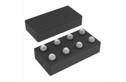
CDC3RL02YFPR Clock Timer ICS Clock Buffer 2Ch Square/Sine- to-Square Wave Clock
|
|
CDC3RL02YFPR Clock Timer ICS Clock Buffer 2Ch Square/Sine- to-Square Wave Clock
1 Features
2 Applications
3 Description The CDC3RL02 is a two-channel clock fan-out buffer and is ideal for use in portable end-equipment, such as mobile phones, that require clock buffering with minimal additive phase noise and fan-out capabilities. It buffers a single master clock, such as a temperature compensated crystal oscillator (TCXO) to multiple peripherals. The device has two clock request inputs (CLK_REQ1 and CLK_REQ2), each of which enable a single clock output. The CDC3RL02 accepts square or sine waves at the master clock input (MCLK_IN), eliminating the need for an AC coupling capacitor. The smallest acceptable sine wave is a 0.3-V signal (peak-to- peak). CDC3RL02 has been designed to offer minimal channel-to-channel skew, additive output jitter, and additive phase noise. The adaptive clock output buffers offer controlled slew-rate over a wide capacitive loading range which minimizes EMI emissions, maintains signal integrity, and minimizes ringing caused by signal reflections on the clock distribution lines. The CDC3RL02 has an integrated Low-Drop-Out (LDO) voltage regulator which accepts input voltages from 2.3 V to 5.5 V and outputs 1.8 V, 50 mA. This 1.8-V supply is externally available to provide regulated power to peripheral devices such as a TCXO. The CDC3RL02 is offered in a 0.4-mm pitch wafer- level chip-scale (WCSP) package (0.8 mm × 1.6 mm) and is optimized for very low standby current consumption. Device Information
|
||||||
| Product Tags: timer ic chip time delay ic chip |
|
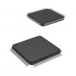
LPC1768FBD100K MCU Chips IC MCU 32BIT 512KB FLASH 100LQFP 32 BIT Micro Controllers |

|
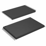
EPCS16SI8N NEW AND ORIGINAL STOCK |
|
Professional Flash Memory Products Ic Memory Chip XCF08PVOG48C |

|
M45PE10-VMN6P Flash Memory IC NEW AND ORIGINAL STOCK |

|
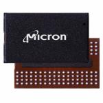
MT49H8M36FM-33 TR NEW AND ORIGINAL STOCK |
|
MT49H32M9FM-25 TR(DQJMT) NEW AND ORIGINAL STOCK |