
CD4066BM96 Ethernet Switch IC Analog Switch ICs Quad
|
|
CD4066BM96 Ethernet Switch IC Analog Switch ICs Quad
1 Features
2 Applications
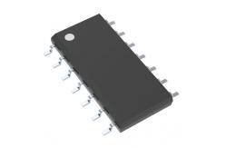
3 Description The CD4066B device is a quad bilateral switch intended for the transmission or multiplexing of analog or digital signals. It is pin-for-pin compatible with the CD4016B device, but exhibits a much lower on-state resistance. In addition, the on-state resistance is relatively constant over the full signal- input range. The CD4066B device consists of four bilateral switches, each with independent controls. Both the p and the n devices in a given switch are biased on or off simultaneously by the control signal. As shown in Figure 17, the well of the n-channel device on each switch is tied to either the input (when the switch is on) or to VSS (when the switch is off). This configuration eliminates the variation of the switch- transistor threshold voltage with input signal and, thus, keeps the on-state resistance low over the full operating-signal range. The advantages over single-channel switches include peak input-signal voltage swings equal to the full supply voltage and more constant on-state impedance over the input-signal range. However, for sample-and-hold applications, the CD4016B device is recommended. Device Information
|
||||||||||||||
| Product Tags: ethernet transceiver ic fast ethernet switch chip |
|
24AA1025-I/SM Programmable IC Chips 1024K I2C™ CMOS Serial EEPROM |
|
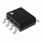
SST26VF032B-104I/MF FLASH Memory IC 32Mbit SPI - Quad I/O 104 MHz 8-WDFN (5x6) |

|
SST26VF032B-104I/MF Flash Memory Chip IC Micro 32 Mbit Low Power Consumption |
|
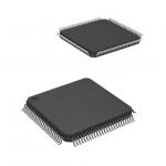
LPC1768FBD100K MCU Chips IC MCU 32BIT 512KB FLASH 100LQFP 32 BIT Micro Controllers |

|
EPCS16SI8N NEW AND ORIGINAL STOCK |
|
Professional Flash Memory Products Ic Memory Chip XCF08PVOG48C |