
SN74LVC2G74DCUR 10 μA Max ICC Programmable Logic ICS Flip Flops Positive Edge Trig
|
|
SN74LVC2G74DCUR Programmable Logic ICS Flip Flops Positive Edge Trig
1 Features
2 Applications
3 Description This single positive-edge-triggered D-type flip-flop is designed for 1.65-V to 5.5-V VCC operation. NanoFreeTM package technology is a major breakthrough in IC packaging concepts, using the die as the package. A low level at the preset (PRE) or clear (CLR) input sets or resets the outputs, regardless of the levels of the other inputs. When PRE and CLR are inactive (high), data at the data (D) input meeting the setup time requirements is transferred to the outputs on the positive-going edge of the clock pulse. Clock triggering occurs at a voltage level and is not related directly to the rise time of the clock pulse. Following the hold-time interval, data at the D input can be changed without affecting the levels at the outputs. This device is fully specified for partial-power-down applications using Ioff. The Ioff circuitry disables the outputs, preventing damaging current backflow through the device when it is powered down. Device Information
|
||||||||||
| Product Tags: programmable computer chip logic integrated circuits |
|
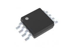
24AA1025-I/SM Programmable IC Chips 1024K I2C™ CMOS Serial EEPROM |
|
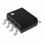
SST26VF032B-104I/MF FLASH Memory IC 32Mbit SPI - Quad I/O 104 MHz 8-WDFN (5x6) |

|
SST26VF032B-104I/MF Flash Memory Chip IC Micro 32 Mbit Low Power Consumption |
|
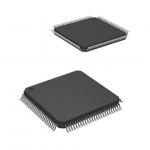
LPC1768FBD100K MCU Chips IC MCU 32BIT 512KB FLASH 100LQFP 32 BIT Micro Controllers |

|
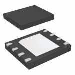
EPCS16SI8N NEW AND ORIGINAL STOCK |
|
Professional Flash Memory Products Ic Memory Chip XCF08PVOG48C |