
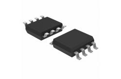
SN74LVC2G125DCTRHigh Speed Programmable Logic ICS Buffers Line Drivers Live Insertion
|
|
SN74LVC2G125DCTR Programmable Logic ICS Buffers & Line Drivers Tri-State Dual Bus
1 Features
2 Applications
3 Description The SN74LVC2G125 device is a dual bus buffer gate, designed for 1.65-V to 5.5-V VCC operation. This device features dual line drivers with 3-state outputs. The outputs are disabled when the associated output-enable (OE) input is high. NanoFreeTM package technology is a major breakthrough in IC packaging concepts, using the die as the package. To ensure the high-impedance state during power up or power down, OE should be tied to VCC through a pullup resistor; the minimum value of the resistor is determined by the current-sinking capability of the driver. This device is fully specified for partial-power-down applications using Ioff. The Ioff circuitry disables the outputs, preventing damaging current backflow through the device when it is powered down. Device Information
|
||||||||||||
| Product Tags: programmable computer chip programmable logic array ic |
|
24AA1025-I/SM Programmable IC Chips 1024K I2C™ CMOS Serial EEPROM |
|
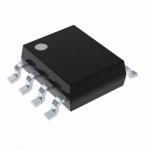
SST26VF032B-104I/MF FLASH Memory IC 32Mbit SPI - Quad I/O 104 MHz 8-WDFN (5x6) |

|
SST26VF032B-104I/MF Flash Memory Chip IC Micro 32 Mbit Low Power Consumption |
|
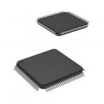
LPC1768FBD100K MCU Chips IC MCU 32BIT 512KB FLASH 100LQFP 32 BIT Micro Controllers |

|
EPCS16SI8N NEW AND ORIGINAL STOCK |
|
Professional Flash Memory Products Ic Memory Chip XCF08PVOG48C |