LTC3851EMS Synchronous Step-Down Switching Regulator Controller
|
|
LTC3851EMSE#PBF Synchronous Step-Down Switching Regulator Controller
FEATURES
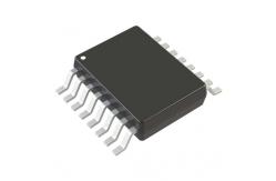
Wide VIN Range: 4V to 38V Operation RSENSE or DCR Current Sensing ±1% Output Voltage Accuracy Power Good Output Voltage Monitor Phase-Lockable Fixed Frequency: 250kHz to 750kHz Dual N-Channel MOSFET Synchronous Drive Very Low Dropout Operation: 99% Duty Cycle Adjustable Output Voltage Soft-Start or Tracking Output Current Foldback Limiting Output Overvoltage Protection OPTI-LOOP® Compensation Minimizes COUT Selectable Continuous, Pulse-Skipping or Burst Mode® Operation at Light Loads Low Shutdown IQ: 20μA VOUT Range: 0.8V to 5.5V n Thermally Enhanced 16-Lead MSOP or 3mm × 3mm QFN Package
APPLICATIONS
Automotive Systems Telecom Systems Industrial Equipment Distributed DC Power Systems
DESCRIPTION
The LTC®3851-1 is a high performance synchronous step-down switching regulator controller that drives an all N-channel synchronous power MOSFET stage. A con stant frequency current mode architecture allows a phase-lockable frequency of up to 750kHz. OPTI-LOOP compensation allows the transient response to be optimized over a wide range of output capacitance and ESR values. The LTC3851-1 features a precision 0.8V reference and a power good indicator. A wide 4V to 38V (40V absolute maximum) input supply range encompasses most battery confi gurations and intermediate bus voltages. The TK/SS pin ramps the output voltage during start-up and shutdown with coincident or ratiometric tracking. Current foldback limits MOSFET heat dissipation during short-circuit conditions. The MODE/PLLIN pin selects among Burst Mode operation, pulse skipping mode or continuous inductor current mode at light loads and allows the IC to be synchronized to an external clock. The LTC3851-1 is identical to the LTC3851 except that the ILIM pin is replaced by PGOOD.
TYPICAL APPLICATION
ABSOLUTE MAXIMUM RATINGS
Input Supply Voltage (VIN) ......................... 40V to –0.3V Topside Driver Voltage (BOOST) ................ 46V to –0.3V Switch Voltage (SW) ..................................... 40V to –5V INTVCC, (BOOST – SW), RUN, PGOOD ........ 6V to –0.3V TK/SS .................................................... INTVCC to –0.3V SENSE+, SENSE– .......................................... 6V to –0.3V MODE/PLLIN, FREQ/PLLFLTR ............... INTVCC to –0.3V
ITH, VFB Voltages .......................................... 3V to –0.3V INTVCC Peak Output Current ..................................50mA Operating Junction Temperature Range (Notes 2, 3) ............................................ –40°C to 125°C Storage Temperature Range ................... –65°C to 150°C Lead Temperature (Soldering, 10 sec) MSE .................................................................. 300°C
PIN CONFIGURATION
ORDER INFORMATION
Hot selling offer!!!
|
|||||||||||||||||||||||||||||||||||||||||||||||||||||||||||||||||||||||||||||||||||||||||||||||||||||||||||||||||||||||||||||||||||||||||||||||||||||||||||||||||||||||||||||||||||||||||||||||||||||||||||||||||||||||||||||||||||||||||||||||||||||||||||||||||||||||||||||||||||||||||||||||||||||||||||||||||||||||||||||||||||||||||||||||||||||||||||||||||||||||||||||||||||||||||||||||||||||||||||||||||||||||||||||||||||||||||||||||||||||||||||||||||||||||||||||||||||||||||||||||||||||||||||||||||||||||||||||||||||||||||||||
| Product Tags: chip in electronics integrated components |