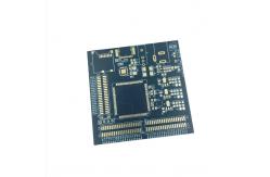
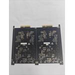
Product Description:
Multilayer PCB Fabrication
Multilayer PCB fabrication is a process used to create multi-level
printed circuit boards and multi-level printed wiring boards. It is
a specialized process that requires a high degree of precision and
accuracy to ensure the highest quality product. The process
involves a variety of steps to achieve the desired result,
including the preparation of the layers, the application of solder
mask, the application of a surface finish, and the application of
silkscreen color.
The silkscreen color available for multilayer PCB fabrication can
include white, black, yellow, and other colors. The solder mask
colors available include green, blue, white, black, red, and other
colors. For the surface finish, HASL, ENIG, OSP, Immersion Silver,
Immersion Tin, and other finishes are available.
In order to ensure the highest quality output, the minimum line
width and minimum line spacing for multilayer PCB fabrication must
be precise. The minimum line width for multilayer PCB fabrication
is typically 0.1mm and the minimum line spacing is also 0.1mm.
Multilayer PCB fabrication is a complex process that requires a
high degree of precision and accuracy in order to ensure the
highest quality product. It is important to work with experienced
professionals who understand the intricacies of the process in
order to produce the desired outcome.
Features:
- Product Name: Multilayer PCB Fabrication
- Solder Mask Color: Green, Blue, White, Black, Red, Etc.
- Min. Hole Size: 0.2mm
- Surface Finish: HASL, ENIG, OSP, Immersion Silver, Immersion Tin, Etc.
- Layer Count: 2-20
- Impedance Control: Yes
- Special Feature: Multi-Layer Printed Circuit Board Production, Multi-Layer Printed
Circuit Board Production, Multi-Level Printed Wiring Board Creation
Technical Parameters:
| Parameter | Specification |
|---|
| Min. Hole Size | 0.2mm |
| Material | FR4, High TG FR4, Halogen Free, Rogers, Etc. |
| Min. Line Spacing | 0.1mm |
| Copper Thickness | 1-4oz |
| Layer Count | 2-20 |
| Impedance Control | Yes |
| Board Thickness | 0.2-3.2mm |
| Silkscreen Color | White, Black, Yellow, Etc. |
| Solder Mask Color | Green, Blue, White, Black, Red, Etc. |
| Min. Line Width | 0.1mm |
Applications:
JIETENG Multi-Layer Printed Circuit Board Production is designed to provide customers with high-level printed circuit
board assembly, multi-level printed circuit board fabrication,
multi-level printed wiring board creation, and multi-level PCB
design and manufacture services. The PCB circuit board model number
is JIETENG-PCB. It is produced in China with various solder mask
colors such as green, blue, white, black, and red. It is suitable
for 2-20 layer counts and has a minimum hole size of 0.2mm. The
copper thickness can range from 1-4oz and the silkscreen color is
available in white, black, and yellow.
This multi-layer printed circuit board production is highly
reliable and cost-effective. It is perfect for applications in
various industries such as consumer electronics, automotive,
medical, and aerospace. It is designed with advanced technology
that meets the most stringent requirements and standards in the
industry. It offers excellent thermal performance and a high level
of signal integrity and reliability.
JIETENG multi-layer printed circuit board production ensures that
customers receive the highest quality products with the shortest
lead time. The boards are manufactured with the highest precision
and accuracy. Our experienced team of engineers provides superior
technical support and ensures that all products meet customer
requirements and industry standards.
Customization:
Customized Multi-Level Printed Circuit Board Fabrication Service
from JIETENG
Brand Name: JIETENG
Model Number: PCB circuit board
Place of Origin: China
Material: FR4, High TG FR4, Halogen Free, Rogers, Etc.
Copper Thickness: 1-4oz
Min. Hole Size: 0.2mm
Silkscreen Color: White, Black, Yellow, Etc.
Min. Line Spacing: 0.1mm
JIETENG is a leading provider of multi-level printed circuit board
fabrication services, offering high quality products and services
for multi-level printed circuit board component assembly,
multi-level printed wiring board creation and more.
Our PCBs are crafted with top-grade materials such as FR4, High TG
FR4, Halogen Free, and Rogers, with copper thicknesses ranging from
1-4oz and minimum hole sizes of 0.2mm. With our advanced equipment
and superior craftsmanship, we ensure a precise and reliable
product every time. We also offer a variety of silkscreen colors,
including white, black, yellow, and more.
Whether you need multi-level printed circuit board fabrication,
component assembly, or printed wiring board creation, JIETENG is
your one-stop solution for all your needs.
Support and Services:
Multilayer PCB Fabrication
Technical Support and Service for Multilayer PCB Fabrication is
provided to ensure the customer get the best possible results from
their investments. Our team of experts is here to help customers
with any issue or question they may have. We are committed to
providing the highest possible level of service and support to our
customers.
We offer a wide range of services such as:
- Design and Layout Services
- Manufacturing and Assembly Services
- Prototype and Production Fabrication Services
- Testing and Quality Control Services
- Repair and Maintenance Services
Our team of experts is available to assist customers with any issue
or question they may have. Our staff is also available to provide
professional advice and guidance on the best way to achieve the
desired results for your project. We strive to provide the highest
level of service and support to ensure customer satisfaction.
Packing and Shipping:
Packaging and Shipping for Multilayer PCB Fabrication:
- Each board will be packed in an anti-static bag in order to protect
it from electrostatic discharge.
- The boards will then be placed into a cardboard box with cushioning
material to prevent them from getting damaged during shipping.
- The box will be sealed with polyester tape and labeled with the
customer's address and contact information.
- The package will be shipped via a tracked courier service in order
to ensure delivery.
FAQ:
- Q: What is Multilayer PCB Fabrication?
- A: Multilayer PCB Fabrication is a process of producing printed
circuit boards with multiple layers of conductive material
separated by a dielectric layer. It is manufactured by JIETENG,
model number PCB circuit board, with origin from China.
- Q: What are the advantages of Multilayer PCB Fabrication?
- A: Multilayer PCB Fabrication offers advantages such as higher
circuit density, smaller size, higher performance, and greater
flexibility. It also increases the reliability and durability of
the circuit board.
- Q: What are the common materials used in Multilayer PCB
Fabrication?
- A: Common materials used in Multilayer PCB Fabrication include copper
foil, dielectric layers, and solder mask. Other materials include
surface finish, silkscreening, and plating.
- Q: What is the process of Multilayer PCB Fabrication?
- A: The process of Multilayer PCB Fabrication includes the steps of
designing the board, etching the copper layer, laminating the
board, drilling the holes, plating the holes, applying the solder
mask, and silkscreening the board.
- Q: What are the common applications of Multilayer PCB Fabrication?
- A: Multilayer PCB Fabrication is commonly used in the fields of
consumer electronics, automotive, medical, and industrial
applications.