
HASL Prototype Printed Circuit Board Assembly Multilayer
|
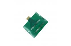
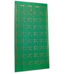
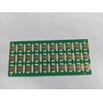
Product Description:Prototype PCB Assembly is a manufacturing process for creating a printed board assembly, which is a board that can be used for a variety of electrical and electronic devices. The printed board assembly is composed of a printed circuit board (PCB) and a variety of components. The PCB is the main component of the printed board assembly, and it is made of a copper-clad laminate. The copper-clad laminate is a kind of metal-based material which is composed of a thin layer of copper and an insulating substrate. The copper layer is etched with a pattern of interconnections to form the printed circuit board. The Prototype PCB Assembly process involves the design and fabrication of a printed circuit board with a variety of components. The components are mounted on the PCB in order to create the desired electrical and electronic circuit. The PCB is then tested and verified to make sure that the circuit works correctly. The PCB is then coated with a solder mask color, which can be green or other colors; this helps to protect the PCB from damage caused by corrosion, heat, and other environmental factors. The Prototype PCB Assembly process requires high precision and accuracy. The PCB must meet certain criteria such as the minimum annular ring of 0.1mm, copper weight of 1oz, minimum line width/space of 0.1mm/0.1mm, and PCB size of 100mm*100mm. By meeting these criteria, the board can be used for a variety of electronic and electrical applications. Features:
Technical Parameters:
Applications:Prototype PCB Assembly Fabrication from JTETENG is the perfect choice for companies in need of reliable, high-quality PCBs. We provide complete PCB fabrication services for prototypes and low-volume PCB production. Our Prototype PCB Assembly Fabrication services provide customers with the highest quality PCB assembly, from FR4 material with HASL surface finish, white silkscreen color and green solder mask color, all with a minimum annular ring of 0.1mm. We offer the most competitive pricing for PCB Fabrication services in China, and the best customer service. Our Prototype PCB Assembly Fabrication services are perfect for those who need high-quality PCBs for their prototypes, and for those who need fast turnaround times. JTETENG provides the best prototype PCB Assembly Fabrication services in China. Customization:JTETENG Prototype PCB Assembly Brand Name: JTETENG Model Number: PCB circuit board Place of Origin: China Min Solder Mask Bridge: 0.1mm Product Name: Prototype PCB Assembly Min Annular Ring: 0.1mm Solder Mask Color: Green Surface Finish: HASL PCB Assembly Manufacturing JTETENG specializes in manufacturing high-quality Prototype PCB Assembly for customers around the world. Our Prototype PCB Assembly fabrication process meets the industry's highest standards to ensure quality and reliability. With our in-house design, engineering, and manufacturing capabilities, we can offer the best in Prototype PCB Assembly fabrication. Prototype PCB Assembly Fabrication JTETENG's Prototype PCB Assembly fabrication process is designed to meet the most demanding requirements of our customers. We use the latest technology and equipment to ensure that our Prototype PCB Assembly meets the highest quality standards. Our experienced staff can help you design and produce the right Prototype PCB Assembly for your unique application. Support and Services:Prototype PCB Assembly Technical Support and Service We provide comprehensive technical support and services for our prototype PCB assembly products. Our experienced team of engineers and technicians are available to help you with any challenges you may face during the assembly process. We can provide advice and assistance on all aspects of the assembly process, including design, testing, and troubleshooting. Our goal is to ensure that your prototype PCB assembly is efficient, reliable, and cost-effective. We also provide a range of services to help make the assembly process as smooth as possible. Our services include:
We take pride in our ability to provide the highest level of customer service and technical support for our prototype PCB assembly products. If you have any questions or concerns, please do not hesitate to contact us. Packing and Shipping:Prototype PCB Assembly Packaging and Shipping: Prototype PCB Assemblies are packaged securely in ESD-protected bags and placed inside a box. All items are protected with appropriate cushioning materials, such as bubble wrap, to ensure their safe arrival at the customer's location. The box is then sealed, labeled with the customer's address, and sent out via the customer's preferred shipping method. FAQ:Q1: What is Prototype PCB Assembly?A1: Prototype PCB Assembly refers to the process of assembling the components onto the printed circuit board (PCB) prototype. It is offered by JTETENG, a China based company. Q2: What components can be used in Prototype PCB Assembly? A2: Prototype PCB Assembly can be used to assemble a variety of components onto the PCB, including resistors, capacitors, transistors, integrated circuits, and other electronic components. Q3: What processes are involved in Prototype PCB Assembly? A3: Prototype PCB Assembly usually involves a few processes, such as component placement, soldering, cleaning, and testing. Q4: How long does the Prototype PCB Assembly take? A4: The time it takes to complete the Prototype PCB Assembly depends on the complexity of the circuit board and the number of components on it. Generally speaking, it usually takes 2-3 days. Q5: What is the quality assurance of Prototype PCB Assembly? A5: JTETENG provides high-quality Prototype PCB Assembly with strict quality control procedures. The products are tested and inspected to ensure they meet the highest standards of quality and performance. |
||||||||||||||||||||||
| Product Tags: multilayer prototype printed circuit board assembly HASL prototype printed circuit board assembly multilayer electronic prototype assembly |
|
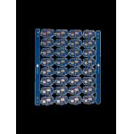
Affordable PCB Prototyping For Automotive Electronics Radar Sensor Thick Copper 2oz |
|
8-Layer Blind Via PCB Prototype Manufacturing Automotive Electronic Sensing |
|
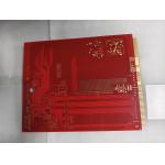
High Precision 3.0mm Thick 8-Layer First-Order HDI Blind Hole Board FR4 HF Material OEM |
|
HASL Immersion Tin Surface Treatment PCB 3.0mm Industrial Camera |

|
Customized Green Halogen Free PCB Assembly Tinning Surface Treatment 3.0MM for Drones |
|
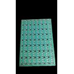
8-Layer FR4 HF Encoder Precision PCB Thickness 3.0mm |