
Rogers OSP Multilayer Pcb Fabrication High Effective
|
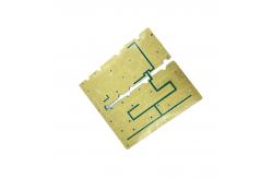
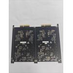
Product Description:Multilayer PCB Fabrication is a comprehensive process for producing multi-layer printed circuit boards (PCBs). This process involves multiple layers of copper-clad laminate and other components, such as solder mask, soldermask, and surface finish. It is highly advanced and requires precise engineering and manufacturing processes for accurate results. The board thickness can range from 0.2mm to 3.2mm, depending on the application. The surface finish can be HASL, ENIG, OSP, immersion silver, immersion tin, and others. The minimum line width is 0.1mm, and the impedance control is available for more complex designs. Various solder mask colors are available, such as green, blue, white, black, and red. This multi-layer PCB fabrication process provides reliable and cost-effective solutions for creating multi-level printed wiring boards. Features:
Technical Parameters:
Applications:JTETENG Multi-Layer PCB Fabrication is the perfect choice for companies looking to create a multi-level printed wiring board. With our PCB circuit boards, you can create up to 20 layers of wiring and components. Our boards feature copper thickness of up to 4oz, and a minimum line width of 0.1mm, allowing for intricate designs. Impedance control is available for those looking to ensure precise signal pathways. Our silkscreen printing colors include white, black, yellow, and more. Our multi-layer PCB fabrication and component assembly services will help you build the perfect board for your purpose. Customization:JTETENG Multi-Layer PCB Fabrication Services JTETENG offers professional Multi-Layer Printed Circuit Board (PCB) Fabrication services. Our Multi-Layer PCBs are designed for high performance, reliability and durability. We specialize in creating Multi-Level Printed Wiring Boards with the following specifications:
Multi-Level Printed Circuit Board Fabrication, Multi-Level Printed Wiring Board Creation and Multi-Layer PCB Component Assembly are just some of the services that JTETENG can provide. Contact us today for more information about our Multi-Layer PCB Fabrication services. Support and Services:Multilayer PCB Fabrication Technical Support and Services We offer technical support and services for Multilayer PCB
Fabrication. Our team of experts can assist you in all aspects of
the production process, from design and engineering to full-scale
fabrication. Packing and Shipping:Packaging and Shipping for Multilayer PCB Fabrication Multilayer PCBs should be packaged and shipped properly to ensure
their safe arrival at their destination. Packaging should be
designed to protect the product from dust, moisture, and other
external factors. All components should be securely packaged and
labeled to ensure proper identification and handling. FAQ:A1: JTETENG Multilayer PCB Fabrication is made of the highest-grade
materials like FR4, polyimide, Aluminum, etc. A2: JTETENG Multilayer PCB Fabrication can reach up to 20 Layers. A3: The minimum line width & space for JTETENG Multilayer PCB
Fabrication is 0.075mm & 0.075mm respectively. A4: The maximum size of a JTETENG Multilayer PCB Fabrication is
505mm x 610mm. A5: JTETENG Multilayer PCB Fabrication is made in China. |
||||||||||||||||||||||
| Product Tags: OSP multilayer pcb fabrication high effective multilayer pcb fabrication OSP rogers pcb fabrication |

|
10-Layer High-Frequency Material FR4 Mixed Pressure Board Is Used For Communication Signal Transmission |

|
Customizable Firefighting Robot Multi-Layer PCB With Black Solder Mask |

|
ENIG Surface Finish Customized Multi-Layer PCB Manufacturing for Communication Equipment Halogen-Free |

|
Industrial Camera Multi-Layer PCB with Halogen-Free Blue Solder Mask and IPC-II Standard |

|
Black Solder Mask Halogen-Free PCB For Industrial Robot Applications |
|
Black Immersion Silver 6-Layer Multi-Layer Circuit Board For CCTV Camera |