Specializing in the production of PCB high-frequency circuit board
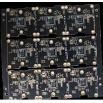
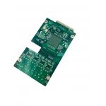
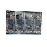
PCBA electronic products development BOM processing Overview Essential details - Model Number:
Pcba 1002
- Type:
Home appliance pcba, Smart Electronic pcba
- Place of Origin:
Guangdong, China
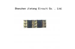
- Brand Name:
JIETENG
- Supplier Type:
PCBA
- Copper Thickness:
1/2OZ 1OZ 2OZ 3OZ
- Name:
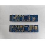
Car GPS Tracker PCBA Manufacturer
- Keywords:
One Stop Service Oem Pcb Assembly
- Number of Layers:
1,2,4,6,up to 26 layers
- Material:
FR-4, glass epoxy, FR4 High Tg, Rohs compliant, Aluminum, Rogers,
etc
- Application:
Electronics Device
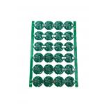
- PCB type:
Hard, flexible, rigid-flexible
- Shape:
Any shape: Rectangular,round,slots,cutouts,complex,irregular, etc
- Board Thickness:
0.4~4.0mm
- PCBA service:
SMD SMT DIP Component Assembly
- Certificate:
ISO9001/Iso14001/CE/ROHS
| Mass production: 2~58 layers / Pilot run: 64 layers | | Mass production: 394mil (10mm) / Pilot run: 17.5mm | | FR-4 (Standard FR4, Mid-Tg FR4,Hi-Tg FR4, Lead free assembly
material) , Halogen-Free, Ceramic filled , Teflon, Polyimide,
BT,PPO, PPE, Hybrid, Partial hybrid, etc. | | Inner layer: 3mil/3mil (HOZ), Outer layer: 4mil/4mil(1OZ) | | UL certificated: 6.0 OZ / Pilot run: 12OZ | | Mechanical drill: 8mil(0.2mm) Laser drill: 3mil(0.075mm) | | 1150mm × 560mm | | 18:1 | | HASL,Immersion Gold, Immersion Tin, OSP, ENIG + OSP, Immersion
Silver, ENEPIG, Gold Finger | | Buried Hole, Blind Hole, Embedded Resistance, Embedded Capacity,
Hybrid, Partial hybrid, Partial high density, Back drilling, and
Resistance control |
| Position accuracy:20 um | Components size:0.4×0.2mm(01005) —130×79mm,Flip-CHIP,QFP,BGA,POP | Max. component height::25mm | Max. PCB size:680×500mm | Min. PCB size:no limited | PCB thickness:0.3 to 6mm | PCB weight:3KG | | Max. PCB width:450mm | Min. PCB width: no limited | Component height:Top 120mm/Bot 15mm | | Metal type :part, whole, inlay, sidestep | Metal material:Copper , Aluminum | Surface Finish:plating Au, plating sliver , plating Sn | | Air bladder rate:less than 20% | Press range:0-50KN | Max. PCB size:800X600mm | | ICT,Probe flying,burn-in,function test,temperature cycling |
|