
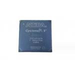
Field Programmable Gate Array IC EP1C6Q240C8N Cyclone EPC6 Series 5980 LABs 185 IOs
|
|
Programmable Gate Arrays EP1C6Q240C8N Cyclone EPC6 Series 598 LABs 185 IOs Specifications
Description Cyclone® devices contain a two-dimensional row- and column-based architecture to implement custom logic. Column and row interconnects of varying speeds provide signal interconnects between LABs and embedded memory blocks.
The logic array consists of LABs, with 10 LEs in each LAB. An LE is a small unit of logic providing efficient implementation of user logic functions. LABs are grouped into rows and columns across the device. Cyclone devices range between 2,910 to 20,060 LEs.
M4K RAM blocks are true dual-port memory blocks with 4K bits of memory plus parity (4,608 bits). These blocks provide dedicated true dual-port, simple dual-port, or single-port memory up to 36-bits wide at up to 250 MHz. These blocks are grouped into columns across the device in between certain LABs. Cyclone devices offer between 60 to 288 Kbits of embedded RAM.
Each Cyclone device I/O pin is fed by an I/O element (IOE) located at the ends of LAB rows and columns around the periphery of the device. I/O pins support various single-ended and differential I/O standards, such as the 66- and 33-MHz, 64- and 32-bit PCI standard and the LVDS I/O standard at up to 640 Mbps. Each IOE contains a bidirectional I/O buffer and three registers for registering input, output, and output-enable signals. Dual-purpose DQS, DQ, and DM pins along with delay chains (used to phase-align DDR signals) provide interface support with external memory devices such as DDR SDRAM, and FCRAM devices at up to 133 MHz (266 Mbps) Features ■ 2,910 to 20,060 LEs, see Table 1–1 ■ Up to 294,912 RAM bits (36,864 bytes) ■ Supports configuration through low-cost serial configuration device ■ Support for LVTTL, LVCMOS, SSTL-2, and SSTL-3 I/O standards ■ Support for 66- and 33-MHz, 64- and 32-bit PCI standard ■ High-speed (640 Mbps) LVDS I/O support ■ Low-speed (311 Mbps) LVDS I/O support ■ 311-Mbps RSDS I/O support ■ Up to two PLLs per device provide clock multiplication and phase shifting ■ Up to eight global clock lines with six clock resources available per logic array block (LAB) row ■ Support for external memory, including DDR SDRAM (133 MHz), FCRAM, and single data rate (SDR) SDRAM ■ Support for multiple intellectual property (IP) cores, including Altera® MegaCore® functions and Altera Megafunctions Partners Program (AMPPSM) megafunctions. Trading Guide
|
||||||||||||||||||||||||||||||||||||||||||||||||||||||
| Product Tags: Gate Array IC EP1C6Q240C8N Programmable Gate Array EP1C6Q240C8N Gate Array IC Cyclone EPC6 |
|
EPM570T144C5N programmable fpga CPLD Complex Programmable Logic Devices 2.5 V 3.3 VTQFP-144 |
|
EP1C6Q240C8 IC CHIP PROGRAMMER EP1C6Q240C8N FPGA FIELD PROGRAMMABLE GATE ARRAY FPGA CYCLONE I 598 LABS 185 IOS |
|
SR1X7- E3827 CPU IC Chips with 3 Working Days Lead Time and Rohs Yes |

|
SR1X7-E3827Program Supply Voltage –2 To 14 V SR1X7 Rohs Yes Best Choice |
|
5CEFA9F23I7N FPGA IC Field Programmable Gate Array 1.5 GHz |
|
Versatile Programmable IC Chips 5CEFA9F23I7N Supply Voltage –2 To 14 V |