
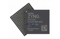
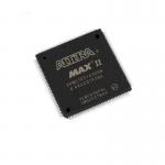
XC7Z020-3CLG400E Programmable IC Chips SoC FPGA Embedded Processors And Controller Chip
|
|
Zynq-7000 SoC XC7Z020-3CLG400E Field Programmable Gate Array FPGA Embedded Processors And Controller Chip
Applications • Automotive driver assistance, driver information, and
infotainment • Video and night vision equipment
Specifications
Description Zynq-7000 SoC First Generation Architecture The Zynq®-7000 family is based on the Xilinx SoC architecture. These products integrate a feature-rich dual-core or single-core ARM® Cortex™-A9 based processing system (PS) and 28 nm Xilinx programmable logic (PL) in a single device. The ARM Cortex-A9 CPUs are the heart of the PS and also include on-chip memory, external memory interfaces, and a rich set of peripheral connectivity interfaces.
Features ARM Cortex-A9 Based Application Processor Unit (APU) • 2.5 DMIPS/MHz per CPU • CPU frequency: Up to 1 GHz • Coherent multiprocessor support • ARMv7-A architecture • TrustZone® security • Thumb®-2 instruction set • Jazelle® RCT execution Environment Architecture • NEON™ media-processing engine • Single and double precision Vector Floating Point Unit (VFPU) • CoreSight™ and Program Trace Macrocell (PTM) • Timer and Interrupts • Three watchdog timers • One global timer • Two triple-timer counters On-Chip Memory • On-chip boot ROM • 256 KB on-chip RAM (OCM) • Byte-parity support External Memory Interfaces • Multiprotocol dynamic memory controller • 16-bit or 32-bit interfaces to DDR3, DDR3L, DDR2, or LPDDR2 memories • ECC support in 16-bit mode • 1GB of address space using single rank of 8-, 16-, or 32-bit-wide memories • Static memory interfaces • 8-bit SRAM data bus with up to 64 MB support • Parallel NOR flash support • ONFI1.0 NAND flash support (1-bit ECC) • 1-bit SPI, 2-bit SPI, 4-bit SPI (quad-SPI), or two quad-SPI (8-bit) serial NOR flash 8-Channel DMA Controller • Memory-to-memory, memory-to-peripheral, peripheral-to-memory, and scatter-gather transaction support I/O Peripherals and Interfaces • Two 10/100/1000 tri-speed Ethernet MAC peripherals with IEEE Std 802.3 and IEEE Std 1588 revision 2.0 support • Scatter-gather DMA capability • Recognition of 1588 rev. 2 PTP frames • GMII, RGMII, and SGMII interfaces • Two USB 2.0 OTG peripherals, each supporting up to 12 Endpoints • USB 2.0 compliant device IP core • Supports on-the-go, high-speed, full-speed, and low-speed modes • Intel EHCI compliant USB host • 8-bit ULPI external PHY interface • Two full CAN 2.0B compliant CAN bus interfaces • CAN 2.0-A and CAN 2.0-B and ISO 118981-1 standard compliant • External PHY interface • Two SD/SDIO 2.0/MMC3.31 compliant controllers • Two full-duplex SPI ports with three peripheral chip selects • Two high-speed UARTs (up to 1 Mb/s) • Two master and slave I2C interfaces • GPIO with four 32-bit banks, of which up to 54 bits can be used with the PS I/O (one bank of 32b and one bank of 22b) and up to 64 bits (up to two banks of 32b) connected to the Programmable Logic • Up to 54 flexible multiplexed I/O (MIO) for peripheral pin assignments Interconnect • High-bandwidth connectivity within PS and between PS and PL • ARM AMBA® AXI based • QoS support on critical masters for latency and bandwidth control Trading Guide
|
||||||||||||||||||||||||||||||||||||||||||||||||||||
| Product Tags: XC7Z020-3CLG400E Programmable IC Chips XC7Z020-3CLG400E SoC FPGA |
|
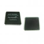
EPM570T144C5N programmable fpga CPLD Complex Programmable Logic Devices 2.5 V 3.3 VTQFP-144 |
|
EP1C6Q240C8 IC CHIP PROGRAMMER EP1C6Q240C8N FPGA FIELD PROGRAMMABLE GATE ARRAY FPGA CYCLONE I 598 LABS 185 IOS |
|
SR1X7- E3827 CPU IC Chips with 3 Working Days Lead Time and Rohs Yes |

|
SR1X7-E3827Program Supply Voltage –2 To 14 V SR1X7 Rohs Yes Best Choice |
|
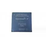
5CEFA9F23I7N FPGA IC Field Programmable Gate Array 1.5 GHz |
|
Versatile Programmable IC Chips 5CEFA9F23I7N Supply Voltage –2 To 14 V |