
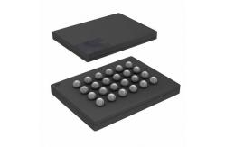
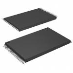
S25FL256SAGBHVB00 IC FLASH 256MBIT SPI/QUAD 24BGA Infineon Technologies
|
Detailed Product Description
Product Details
General DescriptionThe Spansion S25FL128S and S25FL256S devices are flash non-volatile memory products using:■ MirrorBit technology - that stores two data bits in each memory array transistor ■ Eclipse architecture - that dramatically improves program and erase performance ■ 65 nm process lithography
This family of devices connect to a host system via a Serial Peripheral Interface (SPI). Traditional SPI single bit serial input and output (SIngle I/O or SIO) is supported as well as optional two bit (Dual I/O or DIO) and four bit (Quad I/O or QIO) serial commands. This multiple width interface is called SPI Multi-I/O or MIO. In addition, the FL-S family adds support for Double Data Rate (DDR) read commands for SIO, DIO, and QIO that transfer address and read data on both edges of the clock.The Eclipse architecture features a Page Programming Buffer that allows up to 128 words (256 bytes) or 256 words (512 bytes) to be programmed in one operation, resulting in faster effective programming and erase than prior generation SPI program or erase algorithms.Executing code directly from flash memory is often called Execute-In-Place or XIP. By using FL-S devices at the higher clock rates supported, with QIO or DDR-QIO commands, the instruction read transfer rate can match or exceed traditional parallel interface, asynchronous, NOR flash memories while reducing signal count dramatically. The S25FL128S and S25FL256S products offer high densities coupled with the flexibility and fast performance required by a variety of embedded applications. They are ideal for code shadowing, XIP, and data storage.
Features■ Density– 128 Mbits (16 Mbytes) – 256 Mbits (32 Mbytes) ■ Serial Peripheral Interface (SPI) – SPI Clock polarity and phase modes 0 and 3 – Double Data Rate (DDR) option – Extended Addressing: 24- or 32-bit address options – Serial Command set and footprint compatible with S25FL-A, S25FL-K, and S25FL-P SPI families – Multi I/O Command set and footprint compatible with S25FL-P SPI family ■ READ Commands – Normal, Fast, Dual, Quad, Fast DDR, Dual DDR, Quad DDR – AutoBoot - power up or reset and execute a Normal or Quad read command automatically at a preselected address – Common Flash Interface (CFI) data for configuration information. ■ Programming (1.5 Mbytes/s) – 256 or 512 Byte Page Programming buffer options – Quad-Input Page Programming (QPP) for slow clock systems ■ Erase (0.5 to 0.65 Mbytes/s) – Hybrid sector size option - physical set of thirty two 4-kbyte sectors at top or bottom of address space with all remaining sectors of 64 kbytes, for compatibility with prior generation S25FL devices – Uniform sector option - always erase 256-kbyte blocks for software compatibility with higher density and future devices. ■ Cycling Endurance – 100,000 Program-Erase Cycles on any sector typical ■ Data Retention – 20 Year Data Retention typical ■ Security features – One Time Program (OTP) array of 1024 bytes – Block Protection: – Status Register bits to control protection against program or erase of a contiguous range of sectors. – Hardware and software control options – Advanced Sector Protection (ASP) – Individual sector protection controlled by boot code or password ■ Spansion® 65 nm MirrorBit Technology with Eclipse™ Architecture ■ Core Supply Voltage: 2.7V to 3.6V ■ I/O Supply Voltage: 1.65V to 3.6V – SO16 and FBGA packages ■ Temperature Range: – Industrial (-40°C to +85°C) – Automotive In-Cabin (-40°C to +105°C) ■ Packages (all Pb-free) – 16-lead SOIC (300 mil) – WSON 6 x 8 mm – BGA-24 6 x 8 mm – 5 x 5 ball (FAB024) and 4 x 6 ball (FAC024) footprint options – Known Good Die and Known Tested Die
Specifications
DescriptionsFLASH - NOR Memory IC 256Mb (32M x 8) SPI - Quad I/O 133MHz 24-BGA
(6x8) Flash Memory |
Related Products
|
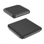
CY7C138-25JXI IC SRAM 32KBIT PARALLEL 68PLCC Cypress Semiconductor Corp |
|
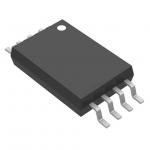
IS25LD020-JDLE IC FLASH 2MBIT SPI 100MHZ 8TSSOP ISSI, Integrated Silicon Solution Inc |
|
DS3065W-100# IC NVSRAM 8MBIT PARALLEL 256BGA Analog Devices Inc./Maxim Integrated |
|
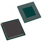
M29W160EB70N6E IC FLASH 16MBIT PARALLEL 48TSOP Micron Technology Inc. |
|
STK11C68-5L55M IC NVSRAM 64KBIT PARALLEL 28LCC Cypress Semiconductor Corp |
|
AT28HC256-90DM/883 IC EEPROM 256KBIT PAR 28CERDIP Microchip Technology |
Email to this supplier