
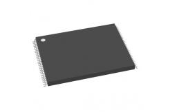
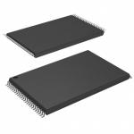
MT29F1G08ABAEAWP-IT:E TR IC FLASH 1GBIT PARALLEL 48TSOP I Micron Technology Inc.
|
Detailed Product Description
Product Details
General DescriptionMicron NAND Flash devices include an asynchronous data interface for high-performance I/O operations. These devices use a highly multiplexed 8-bit bus (I/Ox) to transfer commands, address, and data. There are five control signals used to implement the asynchronous data interface: CE#, CLE, ALE, WE#, and RE#. Additional signals control hardware write protection and monitor device status (R/B#).This hardware interface creates a low pin-count device with a standard pinout that remains the same from one density to another, enabling future upgrades to higher densi ties with no board redesign. A target is the unit of memory accessed by a chip enable signal. A target contains one or more NAND Flash die. A NAND Flash die is the minimum unit that can independently execute commands and report status. A NAND Flash die, in the ONFI specification, is referred to as a logical unit (LUN). There is at least one NAND Flash die per chip enable signal. For further details, see Device and Array Organization. This device has an internal 4-bit ECC that can be enabled using the GET/SET features. See Internal ECC and Spare Area Mapping for ECC for more information.
Features• Open NAND Flash Interface (ONFI) 1.0-compliant1• Single-level cell (SLC) technology • Organization – Page size x8: 2112 bytes (2048 + 64 bytes) – Page size x16: 1056 words (1024 + 32 words) – Block size: 64 pages (128K + 4K bytes) – Plane size: 2 planes x 2048 blocks per plane – Device size: 4Gb: 4096 blocks; 8Gb: 8192 blocks 16Gb: 16,384 blocks • Asynchronous I/O performance – tRC/tWC: 20ns (3.3V), 25ns (1.8V) • Array performance – Read page: 25µs 3 – Program page: 200µs (TYP: 1.8V, 3.3V)3 – Erase block: 700µs (TYP) • Command set: ONFI NAND Flash Protocol • Advanced command set – Program page cache mode4 – Read page cache mode 4 – One-time programmable (OTP) mode – Two-plane commands 4 – Interleaved die (LUN) operations – Read unique ID – Block lock (1.8V only) – Internal data move • Operation status byte provides software method for detecting – Operation completion – Pass/fail condition – Write-protect status • Ready/Busy# (R/B#) signal provides a hardware method of detecting operation completion • WP# signal: Write protect entire device • First block (block address 00h) is valid when ship ped from factory with ECC. For minimum required ECC, see Error Management. • Block 0 requires 1-bit ECC if PROGRAM/ERASE cycles are less than 1000 • RESET (FFh) required as first command after power-on • Alternate method of device initialization (Nand_In it) after power up (contact factory) • Internal data move operations supported within the plane from which data is read • Quality and reliability – Data retention: 10 years – Endurance: 100,000 PROGRAM/ERASE cycles • Operating voltage range – VCC: 2.7–3.6V – VCC: 1.7–1.95V • Operating temperature: – Commercial: 0°C to +70°C – Industrial (IT): –40ºC to +85ºC • Package – 48-pin TSOP type 1, CPL2 – 63-ball VFBGA
Specifications
|
Related Products
|
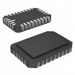
CY7C138-25JXI IC SRAM 32KBIT PARALLEL 68PLCC Cypress Semiconductor Corp |
|
IS25LD020-JDLE IC FLASH 2MBIT SPI 100MHZ 8TSSOP ISSI, Integrated Silicon Solution Inc |
|
DS3065W-100# IC NVSRAM 8MBIT PARALLEL 256BGA Analog Devices Inc./Maxim Integrated |
|
M29W160EB70N6E IC FLASH 16MBIT PARALLEL 48TSOP Micron Technology Inc. |
|
STK11C68-5L55M IC NVSRAM 64KBIT PARALLEL 28LCC Cypress Semiconductor Corp |
|
AT28HC256-90DM/883 IC EEPROM 256KBIT PAR 28CERDIP Microchip Technology |
Email to this supplier