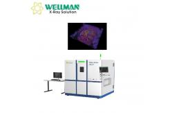
High-Efficiency 3D X Ray Inspection for Large-Sized PCBAs and SMT
Solder Joints Equipment Features - Full 3D automatic imaging and analysis
- Applicable for both on-line inspection and off-line analysis
- Capable of achieving fast CT imaging, with the fastest local
imaging time less than 3 seconds
- Solves the problem of solder joint defect inspection that cannot be
achieved by traditional 2D and 2.5D equipment
- Can be connected to the user's database to directly import
inspection results
Inspection Applications - Large-sized PCBA boards
- The internal structure quality of semiconductor packaging products
- The welding quality of various types of SMT solder joints,
including open soldering, wetting conditions, solder volume,
offset, foreign objects, bridging, and the presence of pins
Equipment Performance Parameters | Parameter | Specification |
|---|
| Maximum possible sample size | 750 mm*530 mm (Length x Width) | | Maximum imaging area | 730 mm*510 mm (Length x Width) | | JIMA card resolution | 4μm | | Equipment weight | 5T | | Equipment size | 2336 mm*2321 mm*2109 mm (Length * width * height) | | Imaging software system | A set of online plate CT imaging system, including integrated
scanning, data analysis and other modules |
Detector Parameters | Parameter | Specification |
|---|
| Detector type | Amorphous silicon flat panel detector | | Pixel size | 49.8 μm | | Pixel matrix | 2304*2813 | | Effective imaging area | 115 mm*140 mm | | Picture frame rate | 18 fps (1*1) |
X-ray Source Parameters | Parameter | Specification |
|---|
| X-ray Tube Type | Closed-tube X-ray source | | Tube voltage range | 45-130 KV | | Tube current range | 0-0.5 mA | | Maximum operating power | 65W |
|