
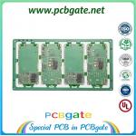
4-Layer HDI PCB for RFID | High-Gain RF Interconnect Solution
|


|
4-Layer HDI PCB for RFID | High-Gain RF Interconnect Solution Product Overview: Our 4-layer HDI PCBs are optimized for high-gain RFID readers and active smart tracking systems. By utilizing a sophisticated 4-layer stack-up with precision micro-via technology, we provide superior electromagnetic shielding and low-loss signal paths essential for long-range RF communication. These boards are designed to support complex NFC controllers and multi-protocol RFID modules in a compact form factor. Featuring excellent dielectric stability, our HDI boards ensure consistent antenna performance and high-speed data processing for industrial IoT and secure access control applications. Key Selling Points: • Enhanced Range: 4-layer shielding for superior RF signal gain. • Compact Layout: High-density micro-vias for small-footprint designs. • Low Interference: Optimized stack-up for minimized EMI/EMC noise. Engineering Support: DFM (Design for Manufacturing) check before production. Testing: Flying Probe Test, Fixture Test, Impedance Control Test, Thermal Stress Test. “ Instant PCB(1-38 layers)”--PCBgate PCBgate is a professional PCB manufacturer providing high-quality printed circuit boards for global electronics industries. We are capable of manufacturing a wide range of PCB types to meet different application requirements, including:FR-4 PCBs,ceramic PCBs,carbon oil PCBs,Aluminum PCBs,Flexible & Rigid-Flex PCBs. We specialize in 4-layer HDI RFID PCB manufacturing, providing the perfect balance between multi-layer signal isolation and space efficiency. By using Laser Direct Imaging (LDI) and high-speed laser drilling, we achieve the precise registration required for your advanced RF impedance and antenna matching designs.
This 4-layer structure is ideal for active RFID tags, high-speed NFC readers, and IoT gateways. We ensure 100% E-test and AOI inspection to guarantee that every board meets the highest industrial standards for signal stability and durable performance.
We support HDI PCB prototypes, small-batch production, and mass production to meet different customer requirements, helping you accelerate your product's time-to-market. Our PCB manufacturing capability includes: • Fine Line Technology: Min. Trace/Space down to 0.075mm / 0.075mm • Blind & Buried Vias: Professional via-in-pad and resin filling processes • High-End Materials: High-TG, Low-Loss, and Halogen-free laminates • Surface Finishes: ENIG, ENEPIG, and OSP for superior soldering • Complex Stack-ups: Multilayer HDI integration up to 20+ layers • Rigorous Testing: AOI, Micro-sectioning, and Impedance Control Attention: pictures are for reference only. The specific products are subject to the original factory model. Standard Packaging: Inner Vacuum Packaging + Outer Carbon Box. Delivery Partners: EMS,DHL,SF-express, FedEx, UPS or Sea/Air Freight for bulk orders. • 15 years of experience in PCB manufacturing. • Advanced Equipment: Equipped with high-speed CNC drilling machines and AOI testing lines. • Professional engineering support • Fast prototype delivery • Global customers from Europe, USA and Asia • Own Global Supply System. • Fast and safe way by EMS/DHL/SF-express/Fedex,etc. • New styles updating everyday and MOQ for all the styles; 1. What's your MOQ and what is PCBgate's fastest delivery time? A: Our MOQ is Minimum packaging quantity, please contact us for details. Sample to mass production all can be supported by PCBgate.
2. Which payment terms does PCBgate accept? A:Advance T/T,Western Union,Paypal, L/C,Credit Card, Cheque,Money Gram and Others.
3.What files are required for PCB quotation? A:Gerber files, PCB specifications and quantity.
4. How to test PCB boards? A: AOI, Fly probe testing, Text fixture testing, FOC etc. For bare PCB. Shipping Information
Welcome to send us your PCB Gerber files for quotation. Our engineering team will respond within 24 hours. |

|
Ultra-Miniature 4-Layer HDI PCB: Advanced Hearing Aid Solution |

|
RFID Precision 2-Layer HDI PCB: High-Sensitivity Smart Tag Core |

|
Precision 6-Layer HDI PCB | Ultra-Compact Hearing Aid Design |

|
Medical-Grade 4-Layer HDI PCB: High-Precision Device Solution |

|
High-Density 4-Layer HDI PCB | Immersion Gold & Blind/Buried Vias |
|
EV Charger Control PCB | 4-Layer HDI Power Management Board |