About TECircuit Found: TECircuit has been operating since 2004.
Location: An electronics manufacturing service(EMS) provider located in
Shenzhen China.
Item: Customizable EMS PCB, offers a full range of one-stop shop services.
Service: Printed Circuit Board (PCB)and Printed Circuit Board Assembly(PCBA), Flexible Printed Circuit Board(FPC), Components Sourcing, Box-Building, Testing.
Quality Assurance: UL,ISO 9001, ISO 14001, ISO 13485, ITAF 16949 andcomplied with ROHS and REACH.
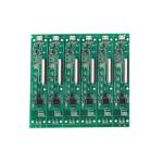
Factory Pictures:
Company's own plant : 50,000 sqm; Employees : 930+; Monthly
production capacity : 100,000 m2 PCBA Applications Remote Design and Manufacturing Control: The PCBA combines broadband internet connectivity with AR
visualization and laser engraving control, enabling operators to
remotely access, modify, and execute engraving jobs from anywhere
in the world through integrated cable or DSL modem functionality. On-Site Industrial Marking with Cloud Integration: Deployed in field service and distributed manufacturing
environments, the device allows technicians to receive complex
engraving designs directly from cloud servers via high-speed
internet, overlay them onto workpieces through AR, and execute
precision marking without returning to a central facility. Real-Time Collaborative Prototyping: Enables distributed design teams to simultaneously view,
annotate, and modify engraving patterns projected onto physical
objects during video conferences, with the PCBA managing
low-latency data synchronization and real-time AR updates across
multiple locations. Smart Factory and Industry 4.0 Integration: Serves as an IIoT node in connected manufacturing environments,
continuously reporting engraving job status, material usage, and
equipment diagnostics to central production management systems
while receiving updated work instructions via cable/DSL
connectivity. Remote Training and Expert Assistance: Allows experienced operators to guide trainees through complex
engraving procedures from remote locations, with the PCBA
transmitting live first-person AR views and receiving annotated
instructions over broadband internet connections. Mobile Field Service and Emergency Repairs: Provides field technicians with immediate access to technical
documentation, video tutorials, and remote expert guidance for
on-site engraving and marking tasks, leveraging built-in modem
connectivity where Wi-Fi is unavailable. Distributed Manufacturing Network Coordination: Powers a network of AR-guided laser engraving stations that
receive and execute jobs from a central dispatch system, with the
PCBA managing job queuing, priority handling, and real-time status
updates across multiple units.
PCBA Features Integrated Cable/DSL Broadband Modem Chipset: The PCBA incorporates a complete cable or DSL modem front-end
with integrated MAC/PHY layers, supporting high-speed data
transmission over existing coaxial or telephone infrastructure for
reliable internet connectivity in industrial and remote locations . High-Performance SoC with Neural Processing Unit (NPU) : Features a powerful system-on-chip with dedicated NPU to
simultaneously manage broadband data routing, real-time AR graphics
rendering, computer vision for workpiece recognition, and precise
laser path calculations with minimal latency . Laser Driver and Safety Interlock System : Integrates microcontroller-based laser control circuits with
multiple redundant safety sensors (lid position, motion detection,
emergency stops) that immediately disable the laser if safety
parameters are violated, ensuring operator protection . Miniature AR Display Engine : Incorporates specialized display drivers for high-brightness
micro-OLED projectors coupled with precision waveguide optics,
ensuring engraved design overlays remain clearly visible under
various ambient lighting conditions . Multi-Sensor Fusion for Spatial Registration : Combines data from integrated cameras, depth sensors, and 6-axis
IMUs through sensor fusion algorithms to achieve sub-millimeter
alignment between virtual engraving patterns and physical
workpieces regardless of surface geometry . Gigabit Ethernet and Wi-Fi 6/7 Connectivity : Provides comprehensive networking options including Gigabit
Ethernet ports for wired backbone connections and tri-band Wi-Fi
6/7 for wireless flexibility, ensuring robust data transfer for
large design files and real-time collaboration . Multi-Layer High-Density Interconnect (HDI) Construction : The PCBA utilizes advanced HDI technology with micro-vias and
multiple layers to integrate broadband modem, laser control, AR
processing, and power management within a compact, wearable form
factor suitable for extended use . Advanced Power Management IC (PMIC) with Battery Backup : Employs a sophisticated PMIC and Battery Management System that
seamlessly switches between AC power, PoE, and internal battery
backup while managing the high current demands of both laser
operation and broadband data transmission . Distributed Processing Architecture : Features a multi-chip design that separates modem data routing,
AR graphics rendering, and laser motion control across dedicated
processors, optimizing thermal distribution and ensuring responsive
performance even during complex networked operations . Industrial-Grade Environmental Protection : The PCBA is conformally coated and uses ruggedized components
rated for extended temperature ranges, vibration resistance, and
protection against dust and moisture, ensuring reliable operation
in demanding industrial environments.
FAQ Question 1: What is needed for a quotation?
Answer:
PCB: QTY, Gerber file, and Technical Requirements( material/surface
finish treatment/copper thickness/board thickness,...)
PCBA: PCB information, BOM,(Testing documents...)
Q2: What file formats do you accept for production?
Answer:
PCB Gerber file
BOM list for PCB
Test method for PCBA
Q3: Are my files safe?
Answer:
Your files are held completely safe and secure. We protect the IP
for our customers in the whole process. All documents from
customers are never shared with any 3rd parties.
Q4: What is the shipment method?
Answer:
We can offer FedEx /DHL / TNT / UPS for shipment. Also, customer
provided shipment method is acceptable.
Q5: What is the payment method?
Answer:
Telegraphic Transfer in advance (Advance TT, T/T), PayPal is
acceptable. PCB & PCBA Description | PCB Assembly OEM Service | | Electronic Components Material Purchasing | | Bare PCB Fabrication | | Cable, Wire-harness Assembly, Sheet Metal, Electrical Cabinet
Assembly Service | | PCB Assembly Service: SMT, BGA, DIP | | PCBA test: AOI, In-Circuit Test (ICT), Functioal Test (FCT) | | Conformal Coating Service | | Prototyping and Mass Production |
| PCBA ODM service | | PCB Layout, PCBA Design According To Your Idea | | PCBA Copy/Clone | | Digital Circuit Design / Analog Circuit Design/ lRF Design
/Embedded Software Design | | Firmware and Microcode Programming Windows Application (GUI)
Programming/Windows Device Driver (WDM) Programming | | Embedded User Interface Design / lSystem Hardware Design |
|