
Multilayer Rigid HDI PCB Printed Circuit Board Tablet Computer Electronics Manufacturing
|
|
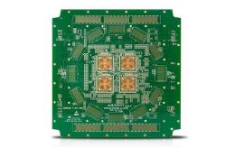
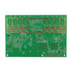
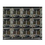
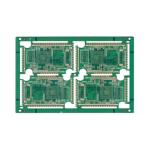
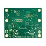
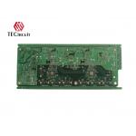
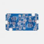
Product Images
About TECircuit
Found: TECircuit has been operating since 2004.
Product Applications
Product Features
FAQ Question 1: What is needed for a quotation? Product Description
|
||||||||||||||||||||||||||||||||||||||||||||||||||||||||||||||||||||||||||||||||||||||||||||||||||||||||||||||||||||||||||||||||||||||||||||||||||||||||||||
| Product Tags: Multilayer Rigid HDI PCB Board Electronics Manufacturing Rigid HDI PCB Computer Manufacturing Printed Circuit Board | ||||||||||||||||||||||||||||||||||||||||||||||||||||||||||||||||||||||||||||||||||||||||||||||||||||||||||||||||||||||||||||||||||||||||||||||||||||||||||||
|
Multilayer HDI PCB Rigid PCB Printed Circuit Board For Smart Weather Station |
|
Multilayer HDI PCB Manufacturer Rigid Printed Circuit Board For Portable Game Console |
|
Multilayer High Density Interconnect Pcb Rigid Printed Circuit Board For Laser Rangefinder |
|
HDI PCB Design Multilayer Rigid Printed Circuit Board For Wireless Network Adapter |
|
Rigid HDI Multilayer PCB Printed Circuit Board For Smart Fitness Equipment |
|
Multilayer HDI PCB Electronics Manufacturing Rigid Printed Circuit Board For Smart Coffee Machine |