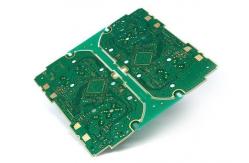
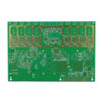
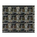
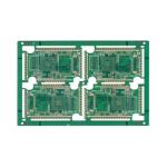
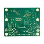
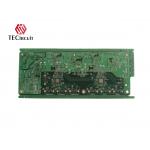
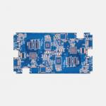
Product Images
About TECircuit Found: TECircuit has been operating since 2004.
Location: An electronics manufacturing service(EMS) provider located in
Shenzhen China.
Item: Customizable EMS PCB, offers a full range of one-stop shop services.
Service: Printed Circuit Board (PCB)and Printed Circuit Board Assembly(PCBA), Flexible Printed Circuit Board(FPC), Components Sourcing, Box-Building, Testing.
Quality Assurance: UL,ISO 9001, ISO 14001, ISO 13485, ITAF 16949 andcomplied with ROHS and REACH.
Factory Pictures:
Company's own plant : 50,000 sqm; Employees : 930+; Monthly
production capacity : 100,000 m2 Product Applications Diagnostic Equipment: - Used in medical imaging devices such as MRI machines and ultrasound
systems, where high precision and reliability are crucial.
Patient Monitoring Systems: - Employed in vital sign monitors that track heart rate, blood
pressure, and other critical health metrics, ensuring accurate data
collection.
Therapeutic Devices: - Integrated into devices like infusion pumps and dialysis machines,
where precise control and monitoring of fluid delivery are
essential.
Wearable Health Devices: - Used in smartwatches and fitness trackers that monitor health
parameters such as heart rate, activity levels, and sleep patterns.
Surgical Instruments: - Employed in advanced surgical devices, ensuring reliable
performance and precision during procedures.
Laboratory Equipment: - Integrated into analytical instruments used in laboratories for
tests and diagnostics, providing accurate results.
Pediatric and Neonatal Equipment: - Used in specialized devices for infants and children, where compact
design and high reliability are critical.
Telemedicine Devices: - Employed in remote monitoring systems that transmit health data to
healthcare providers for analysis and intervention.
Electrocardiogram (ECG) Machines: - Used in ECG devices for monitoring heart activity, where signal
integrity and accuracy are paramount.
Imaging Systems: - Integrated into X-ray and CT scan machines, where high-density
interconnects support complex imaging algorithms.
Product Features High Density: - HDI (High-Density Interconnect) PCBs allow for compact designs with
a high number of components, crucial for space-constrained medical
devices.
Improved Signal Integrity: - Shorter traces and optimized routing enhance signal quality,
essential for accurate data transmission in diagnostic and
monitoring equipment.
Better Thermal Management: - Advanced materials and multilayer designs facilitate effective heat
dissipation, maintaining optimal performance during operation.
Enhanced Routing Flexibility: - The use of microvias and buried vias allows for complex circuit
layouts, maximizing the use of limited space in medical devices.
Lightweight Design: - Reduced material usage contributes to lighter devices, improving
portability and ease of use in various medical settings.
Cost Efficiency in Mass Production: - While initial costs may be higher, HDI PCBs can be cost-effective
for large-scale manufacturing due to their performance benefits.
Customizability: - Can be tailored to meet specific medical application requirements,
allowing for unique layouts and configurations.
Durability: - Built to withstand environmental factors and sterilization
processes, ensuring reliable performance in demanding medical
environments.
Regulatory Compliance: - Designed to meet stringent medical industry standards for safety
and performance, ensuring dependable operation in critical
applications.
Ease of Integration: - Compatible with a wide range of components and technologies,
facilitating the incorporation of advanced features in medical
electronics.
FAQ Question 1: What is needed for a quotation?
Answer:
PCB: QTY, Gerber file, and Technical Requirements( material/surface
finish treatment/copper thickness/board thickness,...)
PCBA: PCB information, BOM,(Testing documents...)
Q2: What file formats do you accept for production?
Answer:
PCB Gerber file
BOM list for PCB
Test method for PCBA
Q3: Are my files safe?
Answer:
Your files are held completely safe and secure. We protect the IP
for our customers in the whole process. All documents from
customers are never shared with any 3rd parties.
Q4: What is the shipment method?
Answer:
We can offer FedEx /DHL / TNT / UPS for shipment. Also, customer
provided shipment method is acceptable.
Q5: What is the payment method?
Answer:
Telegraphic Transfer in advance (Advance TT, T/T), PayPal is
acceptable. Product Description | Specification: | | PCB layers: | 1-42layers | | PCB materials: | CEM1, CEM3, Rogers, FR-4, High Tg FR-4, Aluminum Base, Halogen Free | | PCB max. board size: | 620mm*1100mm | | PCB certificate: | RoHS Directive-Compliant | | PCB Thickness: | 1.6 ±0.1mm | | Out Layer Copper Thickness: | 0.5-5oz | | Inner Layer Copper Thickness: | 0.5-4oz | | PCB max. board thickness: | 6.0mm | | Minimum Hole Size: | 0.20mm | | Minimum Line Width/Space: | 3/3mil | | Min. S/M Pitch: | 0.1mm(4mil) | | Plate Thickness and Aperture Ratio : | 30:1 | | Minimum Hole Copper: | 20µm | | Hole Dia. Tolerance(PTH): | ±0.075mm(3mil) | | Hole dia. Tolerance(NPTH): | ±0.05mm (2mil) | | Hole Position Deviation: | ±0.05mm (2mil) | | Outline Tolerance: | ±0.05mm (2mil) | | PCB solder mask: | Black, white, yellow | | PCB surface finished: | HASL Leadfree,Immersion ENIG,Chem Tin,Flash Gold,OSP,Gold
finger,Peelable,Immersion Silver | | Legend: | White | | E-test: | 100% AOI, X-ray, Flying probe test. | | Outline: | Rout and Score/V-cut | | Inspection Standard: | IPC-A-610CCLASSII | | Certificates: | UL (E503048),ISO9001/ISO14001/IATF16949 | | Outgoing Reports: | Final Inspection, E-test, Solderability Test, Micro Section and
More |
|