In the highly sophisticated and competitive semiconductor and
component manufacturing industry, the reliability and performance
of products are of paramount importance. The Customized Temperature
Humidity Climate Chamber is a cutting-edge solution designed to
meet the unique and exacting demands of this sector, providing a
controlled environment for comprehensive testing and optimization. This specialized chamber is dedicated to simulating a wide range of
temperature and humidity conditions that semiconductors and
electronic components will encounter during their lifecycle. It
serves semiconductor manufacturers, component suppliers, research
institutions, and quality control laboratories. The primary
objective is to evaluate the stability, durability, and
functionality of these products under various environmental
stressors. By subjecting semiconductors and components to precise
temperature and humidity levels, manufacturers can identify
potential weaknesses, improve manufacturing processes, and ensure
that their products meet the highest quality and performance
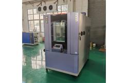
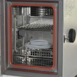
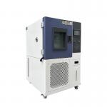
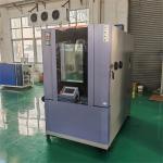
standards. - Ultra-Precise and Stable Construction
- The chamber is constructed with a high-strength, low-outgassing
alloy framework that provides exceptional rigidity and stability.
The interior is lined with a chemically inert and electrostatic
dissipative material to prevent any contamination or damage to the
sensitive semiconductor samples. The door is engineered with a
triple-seal mechanism, incorporating high-precision gaskets and
airlocks, ensuring an ultra-tight and stable testing environment. A
small, optically clear viewing window, made of anti-reflective and
anti-static glass, allows for detailed visual inspection without
compromising the internal conditions. The chamber also features a
vibration isolation system to minimize any external vibrations that
could affect the test results, as even the slightest vibrations can
have a significant impact on the performance of semiconductors.
- Precision Temperature and Humidity Control Systems
- Temperature Control: Capable of maintaining an extremely narrow
temperature range, from -80°C to +200°C, with an astonishing
accuracy of ±0.1°C. It utilizes a combination of cryogenic cooling,
resistive heating, and advanced thermal management technologies.
The control system incorporates a highly sensitive feedback loop,
with multiple platinum resistance temperature detectors (RTDs)
strategically placed within the chamber to ensure uniform
temperature distribution and minimal thermal gradients. The
user-friendly control panel allows for the programming of highly
complex temperature profiles, including rapid temperature ramps,
precise soak times, and cyclic temperature sequences, replicating
real-world scenarios such as the temperature changes during device
operation, storage, and transportation.
- Humidity Control: The humidity control system is equally precise,
capable of achieving humidity levels from 0% to 100% RH (Relative
Humidity), with an accuracy of ±1% RH. It employs a combination of
vapor injection, desiccant dehumidification, and chilled mirror
hygrometry for accurate measurement and control. The chamber is
equipped with a laminar flow system that ensures uniform humidity
distribution and rapid humidity adjustments. High-precision
capacitive humidity sensors continuously monitor the internal
humidity, and the control system makes real-time adjustments to
maintain the desired levels. This is crucial for testing the
effects of moisture on semiconductors, such as the potential for
corrosion, dielectric breakdown, or changes in electrical
properties.
- Advanced Instrumentation and Data Acquisition
- The chamber is outfitted with a comprehensive suite of sensors and
instrumentation. In addition to temperature and humidity sensors,
it includes sensors for measuring electrical parameters such as
leakage current, capacitance, and resistance of the tested
semiconductors and components. These sensors are connected to a
state-of-the-art data acquisition system that records and stores
all relevant data. The data acquisition system offers a high
sampling rate, typically ranging from 1000 to 5000 samples per
second, ensuring that even the most minute and rapid changes in
environmental conditions or product performance are accurately
captured. The collected data can be accessed and analyzed in
real-time or retrieved later for in-depth studies. The system is
also compatible with specialized semiconductor industry data
analysis software, enabling the generation of detailed reports and
graphical representations of the test results, which are essential
for making informed engineering decisions.
- Enhanced Safety and Compliance Features
- The Customized Temperature Humidity Climate Chamber for
Semiconductor and Component Manufacturing is designed with multiple
layers of safety features. It incorporates an automatic emergency
shutdown system that activates immediately in the event of any
critical malfunction, such as overheating, overcooling, or
excessive humidity. The chamber is equipped with a fire suppression
system, which can quickly extinguish any potential fires that may
occur due to electrical faults or chemical reactions. The
ventilation system is engineered to remove any harmful gases or
fumes that may be generated during the testing process, protecting
both the samples and the operators. The control panel is designed
with safety interlocks and clear warning indicators to prevent
accidental operation and ensure the well-being of personnel.
Additionally, the chamber complies with all relevant semiconductor
industry standards and regulations, such as JEDEC standards for
semiconductor testing and IEC 60068 for environmental testing,
ensuring that the testing procedures are recognized and accepted by
regulatory bodies and industry stakeholders, facilitating the
certification and market acceptance of semiconductor products.
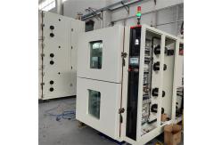
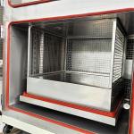
- Chamber Size and Capacity: The chamber is available in a variety of sizes, from small
benchtop models with a volume of a few liters, suitable for testing
individual semiconductor chips or small batches of components, to
larger floor-standing units with volumes up to several cubic
meters, capable of accommodating multiple wafers or larger
assemblies. The interior dimensions are optimized for proper air
circulation and uniform distribution of temperature and humidity,
ensuring that all parts of the tested semiconductors and components
are effectively exposed to the simulated conditions.
- Temperature Cycling Rate: The chamber can perform temperature cycles at a rate of 4 to 8
cycles per hour, depending on the specific requirements of the test
protocol. For example, it can rapidly cool from +120°C to -60°C in
a matter of minutes and then heat back up, subjecting the
semiconductor components to significant thermal stress. The ramp
rate can be adjusted, typically ranging from 1°C per minute to 10°C
per minute, allowing for the simulation of different thermal
profiles.
- Humidity Cycling Rate: The humidity can be cycled within 5 to 15 minutes, allowing for
the simulation of rapid changes in moisture conditions. This
replicates the transitions that may occur, for example, when a
semiconductor device is moved from a dry, controlled manufacturing
environment to a more humid end-user environment or vice versa. The
chamber can quickly adjust the humidity level from a low value,
such as 10% RH, to a high value, such as 90% RH, and back, enabling
the evaluation of the component's response to such changes.
- Data Acquisition Rate: The data acquisition system samples sensor data at a rate of 3000
samples per second, ensuring that even the slightest and most rapid
changes in temperature, humidity, electrical parameters during the
test are accurately recorded. This high sampling rate provides
engineers and scientists with detailed and accurate information
about the performance and behavior of the tested semiconductors and
components, enabling them to identify potential issues and make
informed design improvements.
- Compliance with Industry Standards: The chamber is fully compliant with JEDEC standards, which cover
a wide range of semiconductor testing methods and environmental
stress testing, as well as IEC 60068 for general environmental
testing. This compliance ensures that the testing is conducted in
accordance with the strict requirements and procedures established
by the semiconductor industry, providing confidence in the
reliability and performance of the tested products.
- Accurate Simulation of Semiconductor and Component Operational
Environments
- The primary function of this chamber is to provide a highly
accurate and realistic simulation of the temperature and humidity
conditions that semiconductors and components will face during
their operational lifespan. By precisely controlling temperature
and humidity levels, it allows for the evaluation of how these
products will perform and degrade over time. For example, it can
determine if a semiconductor memory chip will experience data
retention issues in high-temperature and high-humidity conditions
or if a capacitor in an electronic component will have a shortened
lifespan due to moisture-induced corrosion. This information is
invaluable for semiconductor and component manufacturers to
optimize their designs, select appropriate materials, and improve
the overall reliability and durability of their products.
- The ability to conduct repeatable tests with different temperature
and humidity profiles, as mandated by industry standards, is also a
crucial function. This helps in comparing the performance of
various product designs or manufacturing processes and identifying
the most suitable solution. For instance, a semiconductor
manufacturer can test multiple prototypes of a new microprocessor
under the same set of temperature, humidity, and electrical stress
cycling conditions and analyze the results to select the most
reliable and efficient design.
- Enhanced Semiconductor and Component Product Quality and Innovation
- Through comprehensive testing in the Customized Temperature
Humidity Climate Chamber, semiconductor and component product
developers can identify and address potential issues in their
designs. If a component shows signs of failure or degradation
during the test, appropriate measures can be taken, such as
modifying the material composition, improving the manufacturing
process, or adding protective coatings. This leads to the
development of more reliable and durable semiconductor and
component products, reducing the risk of product failures and
enhancing customer satisfaction. In the research and development
field, it allows for the exploration of new materials and
technologies, providing valuable data on their behavior under
extreme temperature and humidity conditions. For example,
researchers can study the performance of new graphene-based
semiconductors in high-temperature and low-humidity environments or
the effectiveness of novel encapsulation materials for protecting
components from moisture.
- The chamber also serves as a powerful tool for quality control. By
subjecting products to standardized environmental tests,
manufacturers can ensure that their products meet the required
quality and performance standards. This helps in building a
reputation for quality and reliability in the highly competitive
semiconductor and component markets, which is essential for winning
customer trust and market share.
- Compliance with Semiconductor and Component Industry Standards and
Regulations
|