
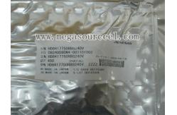
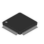
Integrated Circuit Chip HD6417750RBG240 - Renesas Technology Corp - SuperH RISC engine
|
|
Quick Detail:
SuperH RISC engine
Description:
The SH7750 Series (SH7750, SH7750S, SH7750R) is a 32-bit RISC (reduced instruction set computer) microprocessor, featuring object code upward-compatibility with SH-1, SH-2, and SH-3 microcomputers. It includes an instruction cache, an operand cache with a choice of copy-back or write-through mode, and an MMU (memory management unit) with a 64-entry fully-associative unified TLB (translation lookaside buffer). The SH7750 and SH7750S have an 8-kbyte instruction cache and a 16-kbyte data cache. The SH7750R has a 16-kbyte instruction cache and a 32-kbyte data cache. The SH7750 Series has an on-chip bus state controller (BSC) that allows connection to DRAM and synchronous DRAM. Its 16-bit fixed-length instruction set enables program code size to be reduced by almost 50% compared with 32-bit instructions.
Applications:
LSI • Operating frequency: 240 MHz*1, 200 MHz, 167 MHz*2 *3, 133 MHz*2,128 MHz*3 • Performance 432 MIPS (240 MHz), 360 MIPS (200 MHz), 300 MIPS (167 MHz), 240 MIPS (133 MHz), 230 MIPS (128 MHz) 1.7 GFLOPS (240 MHz), 1.4 GFLOPS (200 MHz),1.2 GFLOPS (167 MHz), 0.9 GFLOPS (133 MHz, 128 MHz) • Superscalar architecture: Parallel execution of two instructions • Packages: 256-pin BGA, 208-pin QFP, 264-pin CSP*2 • External buses Separate 26-bit address and 64-bit data buses External bus frequency of 1/2, 1/3, 1/4, 1/6, or 1/8 times internal bus frequency CPU • Original Hitachi SH architecture • 32-bit internal data bus • General register file: Sixteen 32-bit general registers (and eight 32-bit shadow registers) Seven 32-bit control registers Four 32-bit system registers • RISC-type instruction set (upward-compatible with SH Series) Fixed 16-bit instruction length for improved code efficiency Load-store architecture Delayed branch instructions Conditional execution C-based instruction set • Superscalar architecture (providing simultaneous execution of two instructions) including FPU • Instruction execution time: Maximum 2 instructions/cycle • Virtual address space: 4 Gbytes (448-Mbyte external memory space) • Space identifier ASIDs: 8 bits, 256 virtual address spaces • On-chip multiplier • Five-stage pipeline FPU • On-chip floating-point coprocessor • Supports single-precision (32 bits) and double-precision (64 bits) • Supports IEEE754-compliant data types and exceptions • Two rounding modes: Round to Nearest and Round to Zero • Handling of denormalized numbers: Truncation to zero or interrupt generation for compliance with IEEE754 • Floating-point registers: 32 bits × 16 words × 2 banks (single-precision × 16 words or double-precision × 8 words) × 2 banks • 32-bit CPU-FPU floating-point communication register (FPUL) • Supports FMAC (multiply-and-accumulate) instruction • Supports FDIV (divide) and FSQRT (square root) instructions • Supports FLDI0/FLDI1 (load constant 0/1) instructions • Instruction execution times Latency (FMAC/FADD/FSUB/FMUL): 3 cycles (single-precision), 8 cycles (double-precision) Pitch (FMAC/FADD/FSUB/FMUL): 1 cycle (single-precision), 6 cycles (double-precision) Note: FMAC is supported for single-precision only. • 3-D graphics instructions (single-precision only): 4-dimensional vector conversion and matrix operations (FTRV): 4 cycles (pitch), 7 cycles (latency) 4-dimensional vector inner product (FIPR): 1 cycle (pitch), 4 cycles (latency) Clock pulse generator (CPG) • Choice of main clock: SH7750, SH7750S: 1/2, 1, 3, or 6 times EXTAL SH7750R: 1, 6, or 12 times EXTAL • Clock modes: CPU frequency: 1, 1/2, 1/3, 1/4, 1/6, or 1/8 times main clock Bus frequency: 1/2, 1/3, 1/4, 1/6, or 1/8 times main clock Peripheral frequency: 1/2, 1/3, 1/4, 1/6, or 1/8 times main clock Note: Maximum frequency varies with models. • Power-down modes Sleep mode Standby mode Module standby function • Single-channel watchdog timer Memory management unit (MMU) • 4-Gbyte address space, 256 address space identifiers (8-bit ASIDs) • Single virtual mode and multiple virtual memory mode • Supports multiple page sizes: 1 kbyte, 4 kbytes, 64 kbytes, 1 Mbyte • 4-entry fully-associative TLB for instructions • 64-entry fully-associative TLB for instructions and operands • Supports software-controlled replacement and random-counter replacement algorithm • TLB contents can be accessed directly by address mapping Cache memory [SH7750, SH7750S] • Instruction cache (IC) 8 kbytes, direct mapping 256 entries, 32-byte block length Normal mode (8-kbyte cache) Index mode • Operand cache (OC) 16 kbytes, direct mapping 512 entries, 32-byte block length Normal mode (16-kbyte cache) Index mode RAM mode (8-kbyte cache + 8-kbyte RAM) Choice of write method (copy-back or write-through) • Single-stage copy-back buffer, single-stage write-through buffer • Cache memory contents can be accessed directly by address mapping (usable as on-chip memory) • Store queue (32 bytes × 2 entries) Cache memory[SH7750R] • Instruction cache (IC) 16 kbytes, 2-way set associative 256 entries/way, 32-byte block length Cache-double-mode (16-kbyte cache) Index mode SH7750/SH7750S-compatible mode (8 kbytes, direct mapping) • Operand cache (OC) 32 kbytes, 2-way set associative 512 entries/way, 32-byte block length Cache-double-mode (32-kbyte cache) Index mode RAM mode (16-kbyte cache + 16-kbyte RAM) SH7750/SH7750S-compatible mode (16 kbytes, direct mapping) • Single-stage copy-back buffer, single-stage write-through buffer • Cache memory contents can be accessed directly by address mapping (usable as on-chip memory) • Store queue (32 bytes × 2 entries) Interrupt controller(INTC) • Five independent external interrupts: NMI, IRL3 to IRL0 • 15-level encoded external interrupts: IRL3 to IRL0 • On-chip peripheral module interrupts: Priority level can be set for each module Specifications: User break controller (UBC) • Supports debugging by means of user break interrupts • Two break channels • Address, data value, access type, and data size can all be set as break conditions • Supports sequential break function Bus state controller (BSC) • Supports external memory access 64/32/16/8-bit external data bus • External memory space divided into seven areas, each of up to 64 Mbytes, with the following parameters settable for each area: Bus size (8, 16, 32, or 64 bits) Number of wait cycles (hardware wait function also supported) Connection of DRAM, synchronous DRAM, and burst ROM possible by setting space type Supports fast page mode and DRAM EDO Supports PCMCIA interface Chip select signals (&63 to &69) output for relevant areas • DRAM/synchronous DRAM refresh functions Programmable refresh interval Supports CAS-before-RAS refresh mode and self-refresh mode • DRAM/synchronous DRAM burst access function • Big endian or little endian mode can be set Direct memory access controller(DMAC) • Physical address DMA controller: SH7750, SH7750S: 4-channel SH7750R: 8-channel • Transfer data size: 8, 16, 32, or 64 bits, or 32 bytes • Address modes: Single address mode Dual address mode • Transfer requests: External, on-chip module, or auto-requests • Bus modes: Cycle-steal or burst mode • Supports on-demand data transfer Timer unit (TMU) • Auto-reload 32-bit timer: SH7750, SH7750S: 3-channel SH7750R: 5-channel • Input capture function • Choice of seven counter input clocks Realtime clock(RTC) • On-chip clock and calendar functions • Built-in 32 kHz crystal oscillator with maximum 1/256 second resolution(cycle interrupts)Serial communication interface (SCI, SCIF) • Two full-duplex communication channels (SCI, SCIF) • Channel 1 (SCI): Choice of asynchronous mode or synchronous mode Supports smart card interface • Channel 2 (SCIF): Supports asynchronous mode Separate 16-byte FIFOs provided for transmitter and receiver Product lineup Abbreviation Voltage (Internal) Operating Frequency Model No. Package SH7750 1.95 V 200 MHz HD6417750BP200M 256-pin BGA 1.8 V 167 MHz HD6417750F167 HD6417750F167I 1.5 V 128 MHz HD6417750VF128 208-pin QFP SH7750S 1.95 V 200 MHz HD6417750SBP200 256-pin BGA HD6417750SF200 1.8 V 167 MHz HD6417750SF167 HD6417750SF167I 1.5 V 133 MHz HD6417750SVF133 208-pin QFP HD6417750SVBT133 264-pin CSP SH7750R 1.5 V 240 MHz HD6417750RBP240 256-pin BGA HD6417750RF240 208-pin QFP 200 MHz HD6417750RBP200 256-pin BGA HD6417750RF200 208-pin QFP
Specifications:
Competitive Advantage:
Warranty :180 days !
How to buy >>>
Service >>>
|
||||||||||||
| Product Tags: programmable ic chips ic integrated circuits |
|
TL074ACDR Warranty 90Days Shipping by DHL\UPS\Fedex\EMS\Sea\Train ROHS yes Lead time 1-3 Working Days |
|
ESDS312DBVR D/C 22+ Payment Paypal\TT\ Trade Assurance Packaging ESD/Vacuum/Foam/Cartons Warranty 90Days Shipping by DH |
|
AD5664BRMZ-REEL7 Voltage - Supply, Analog 2.7 V ~ 5.5 V Voltage - Supply, Digital 2.7 V ~ 5.5 V INL/DNL (LSB) ±6, ±1 (Ma |
|
ATXMEGA16A4-AU Payment Paypal\TT\ Trade Assurance Packaging ESD/Vacuum/Foam/Cartons Warranty 90Days Shipping by DHL\UPS\ |
|
OPA180IDBVR Lead time 1-3 Working Days Port Shenzhen or HK Package original D/C 22+ Payment Paypal\TT\ Trade Assurance |
|
STM8AF6268TCX EEPROM Size 1K x 8 RAM Size 2K x 8 Voltage - Supply (Vcc/Vdd) 3V ~ 5.5V |