
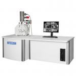
4.5 - 6nm High Magnification Scanning Microscope Electron Surface Topography Eco Sem
|
|
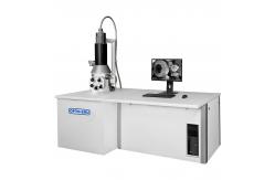
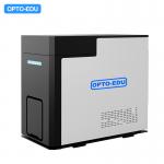
4.5 - 6nm High Magnification Scanning Electron Microscope Surface Topography Eco SEM
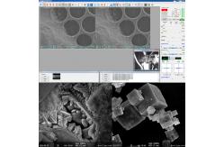
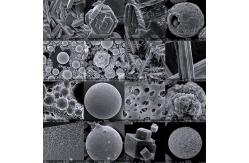
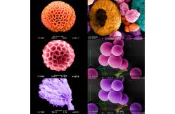
Scanning electron microscopy (sem) is suitable for the observation of the surface topography of metals, ceramics, semiconductors, minerals, biology, polymers, composites and nano-scale one-dimensional, two-dimensional and three-dimensional materials (secondary electron image, backscattered electron image).It can be used to analyze the point, line and surface components of microregion.It is widely used in petroleum, geology, mineral field, electronics, semiconductor field, medicine, biology field, chemical industry, polymer material field, criminal investigation of public security, agriculture, forestry and other fields. Product Description
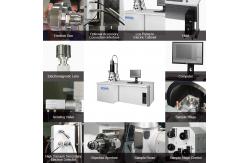
Product Display Optional Accessories
Company Information
OPTO-EDU is one of the top professional supplier for microscope from China, we focus in microscope & educational field for more than 20 years. As the top recommended seller for microsocpe on alibaba, we have full types microscopes, including biological microscope, stereo microscope, metallurgical microscope, inverted microscope, fluorescent microscope, polarizing microscope, phase contrast microscope, dark field microscope, multi-viewing microscope, DIC microscope, AFM/STM/SPM microscope, zoom microscope, gem microscope, digital micoscope, LCD microscope, comparison microscope, forensic microscope, and all kinds of microscope accessories. Our customer comes from more than 104 countries, such as United States, Britain, Russia, Canada, Germany, Denmark, Poland, Sweden, U.A.E., Qatar, Saudi Arabia, Egypt, Mexico, Argentina, Chile, Brazil, Korea, Thailand, India, Indonsia, Philliphine and so on. We have been working tirelessly to supply China's nice quality production to the world market!
|
||||||||||||||||||||||||||||||||||||||||||||||||||||||||
| Product Tags: 6nm scanning microscope electron high magnification scanning microscope electron | ||||||||||||||||||||||||||||||||||||||||||||||||||||||||
|
6x~1000000x Scanning Optical Microscope Digital Five Axis Motorized Stage |
|
OPTO-EDU A63.7005 Schottky Field Emission Scanning Electron Microscope SE BSE 100000x 2.5nm@20KV |

|
OPTO-EDU A63.7004 Single-Crystal Filament Scanning Electron Microscope SE BSE 360000x 3nm@20KV |

|
OPTO-EDU A63.7003 Tungsten Filament Scanning Electron Microscope SE BSE 360000x 4nm@20KV |
|
OPTO-EDU A63.7002 Tungsten Filament Scanning Electron Microscope SE BSE 200000x 6nm@18KV(SE) |
|
OPTO-EDU A63.7001 Tungsten Filament Scanning Electron Microscope SE BSE 150000x 10nm@15KV |